Open Access is an initiative that aims to make scientific research freely available to all. To date our community has made over 100 million downloads. It’s based on principles of collaboration, unobstructed discovery, and, most importantly, scientific progression. As PhD students, we found it difficult to access the research we needed, so we decided to create a new Open Access publisher that levels the playing field for scientists across the world. How? By making research easy to access, and puts the academic needs of the researchers before the business interests of publishers.
We are a community of more than 103,000 authors and editors from 3,291 institutions spanning 160 countries, including Nobel Prize winners and some of the world’s most-cited researchers. Publishing on IntechOpen allows authors to earn citations and find new collaborators, meaning more people see your work not only from your own field of study, but from other related fields too.
To purchase hard copies of this book, please contact the representative in India:
CBS Publishers & Distributors Pvt. Ltd.
www.cbspd.com
|
customercare@cbspd.com
Recent developments in photonic crystal structures have enabled the implementation of optical decoders which possess superior features such as high contrast ratio and fast response. According to published reports, photonic crystal-based decoders exhibit contrast ratios higher than 20 dB and a response time as fast as 200 fs, making them an ideal candidate for high-speed processing applications. Resonant cavities and rings can be utilized to drop waves with high efficiency, thereby simplifying circuits and reducing the need for cross-connections. In this chapter, we provide an introduction to the decoding operation and its importance in various applications, followed by a discussion of fundamental features of photonic crystals such as photonic bandgap and the optical Kerr effect. We also consider the role of resonance in photonic crystals and present recent ideas and designed structures for the benefit of readers.
Department of Electrical Engineering, Shahid Chamran University of Ahvaz, Ahvaz, Iran
Mohammad Soroosh
Department of Electrical Engineering, Shahid Chamran University of Ahvaz, Ahvaz, Iran
Fariborz Parandin
Department of Electrical Engineering, Kermanshah Branch, Islamic Azad University, Kermanshah, Iran
Fatemeh Haddadan
Department of Electrical Engineering, Shahid Chamran University of Ahvaz, Ahvaz, Iran
*Address all correspondence to: mj.maleki@scu.ac.ir
1. Introduction
The need for high-speed processing makes high attention to designing the optical circuits. The wonderful velocity of optical waves in contrast to electrons leads to data transmission via the optical waves as the carriers. Although fast transmission is the main advantage of optical systems, optical confinement is the main challenge to designing optical circuits.
Optical confinement can be achieved by providing a contrast of refractive index between two layers. Optical waveguides are the basic unit of optical circuits and are generally composed of a core that is sandwiched with a clad. In optical circuits, the planar waveguides are composed of three layers including a middle layer with a higher index than other layers. Matching of layers and the quality of interfaces are taking account into the problems that should be solved in preventing power leakage to clad. The lattice constant and doping concentrations of layers play effective roles to design and fabrication of optical waveguides.
In recent years, different types of graphene-based waveguides have been provided with metal-insulator-metal and insulator-metal-insulator structures to guide and control optical waves. Although these structures are designed in a submicron area, the transmission efficiency is not so high to couple in other blocks. Moreover, the transmission efficiency of waveguides depends on the graphene chemical potential that is adjusted with a gate voltage. On the other hand, these waveguides work electro-optically not all-optically. This means that the limitation of electrical switching exists in graphene-based waveguides [1].
All-optical processing is an interesting feature to design optical systems. By realizing all-optical processors, data transmission among the blocks is conducted in an optimum way. Photonic crystal structures have provided a vision for the future to design all-optical optical components of optical processors. Photonic crystals exhibit a photonic bandgap for preventing optical wave propagation at a range of wavelengths. The main concept of the bandgap is caused by the reflection of Bragg layers. Due to a contrast of indices between two adjacent layers, a portion of optical wave amplitude is reflected back, and the construction of some reflections leads to a complete reflector. As a result, a forbidden range of wavelengths for propagation can be obtained in photonic crystals.
High transmission efficiency along with the all-optical mechanisms of the photonic crystal structures makes them a proper medium to design the fundamental blocks in optical processors. Decoders as one of the main blocks in optical circuits have attracted high attention to design based on photonic crystals. The facility of guiding waves in all directions and a wide range of angles is an excellent characteristic of photonic crystal-based decoders. The possibility of guiding the waves in the desired path through resonators helps designers for achieving an optical decoder with high performance.
All-optical processing, simple fabrication process, and high transmission efficiency are the main advantages of the photonic crystal-based decoder in contrast to other structures such as semiconductor optical amplifying, Mach-Zehnder interferometer, and plasmonic decoders. According to the above-mentioned mechanisms for controlling and manipulating the optical waves, the photonic crystal-based structures exhibit a proper medium for achieving the decoding operation. Therefore, the photonic crystal-based decoders are considered in this chapter. Also, some structures with different ideas for designing optical decoders in photonic crystal structures are investigated. The role of the optical Kerr effect and realizing cavity and ring resonators in decoders are also explained in this chapter.
Digital circuits are divided into two categories: combinational circuits and sequential circuits. A combinational circuit is a circuit whose output at any moment depends only on the inputs at that moment. That is, the previous outputs do not affect the current output. On the other hand, a sequential circuit is a circuit whose output depends on the input of the same moment and the previous outputs.
Binary codes can represent discrete data in a digital system. An n-bit binary code can produce up to 2n discrete elements of information. A decoder is a combination circuit that takes binary information from n input lines and converts it to a maximum of 2n output lines [2]. These circuits are shown as n-to-2n decoders.
In an n-input decoder containing 2n outputs, each output is a unique combination of inputs. In some cases, some combinations of input bits may be unused. Therefore, the number of decoder outputs may be less than 2n. For this reason, in some texts, these circuits are called n-to-m decoder, in which m ≤ 2n.
The decoder circuit can also include an enable signal (En). If the enable signal is inactive, the decoder circuit will be disabled and will not function. One of the applications of the decoder is to use it in code converters such as the BCD to 7 segment converters.
Different types of decoders can be designed according to the number of inputs and outputs. Such as decoder 1-to-2, decoder 2-to-4, decoder 3-to-8, and so on. The simplest decoder is a 1-to-2 decoder. This decoder has one input and two outputs. If we denote the input by x and the outputs by D0 and D1, we can say:
If x = 0, then only output D0 is active.
If x = 1, then only output D1 is active.
In a 2-to-4 decoder, the number of inputs is 2 and the number of outputs is 4. The performance of decoders can be shown using the truth table. Figure 1 shows the block diagram of a 2-to-4 decoder [2]. It can be seen in Figure 1 that the inputs are shown by x and y, and the outputs are shown by D0, D1, D2, and D3. The function of this circuit is that if the En port is inactive, all the outputs are inactive, and the decoder does not work.
Figure 1.
(a) A block diagram of 2-to-4 decoder including inputs x and y, outputs D0 to D3, and enable port En [2] (b) the internal circuit of 2-to-4 decoder [2].
The En input must be active for the correct operation of the decoder. In this case, one of the outputs will be activated according to the value of the four input states. The performance of the discussed decoder is shown in Table 1. This table assumes that being active is defined as 1, and being inactive is defined as 0.
Enable
Inputs
Outputs
En
x
y
D3
D2
D1
D0
0
×
×
0
0
0
0
1
0
0
0
0
0
1
1
0
1
0
0
1
0
1
1
0
0
1
0
0
1
1
1
1
0
0
0
Table 1.
The truth table of 2-to-4 decoder. Symbol “×” refers to the do not care state. In this state, the value of the input does not affect the output logic [2].
As can be seen in Table 1, two inputs x and y have four different states. One of the outputs is active for each mode, and the others are inactive. According to the output indices, the output index is equivalent to the binary value of the inputs. In other words, this decoder is a binary-to-decimal converter. Table 1 can be used to design the decoder. Assuming that the activator’s input is En = 1, the outputs can be written according to the input variables as D0 = x’y’, D1 = x’y, D2 = xy’, and D3 = xy.
To design a 2-to-4 decoder, the above-mentioned logic functions can be used and the outputs can be obtained according to the inputs. The obtained circuit is shown in Figure 1b [2].
Two NOT gates in the first column and four AND gates in the second column have been used to design this decoder. In the decoder, only one of the outputs is active at any time, which is determined according to the value of the x and y inputs. NAND gates can also be used to design decoders. In this case, the active state of the outputs is defined as 0. In other words, at any time, only one of the outputs is 0, which is determined according to the binary value of the inputs, and the rest of the outputs are in 1 state.
One of the features of decoders is that a larger decoder can be made using smaller decoders. For example, using two 2-to-4 decoders, you can design a 3-to-8 decoder. The design method of this decoder is shown in Figure 2 [2].
Figure 2.
Designing a 3-to-8 decoder based on two 2-to-4 decoders with the help of enable port [2].
In Figure 2, both inputs of the 2-to-4 decoders are connected to x and y. The third input is created using the En input. In such a way, the complement of this input is connected to the upper decoder (including outputs with a lower value), and this input itself is connected to the lower decoder (including outputs with a higher value).
One of the applications of the decoder is code converter circuits. For example, the decoder can be used in analog to digital converters. In an in-memory system, a decoder can be used to minimize the effect of system decoding.
One of the important uses of the decoder is that it can be used to implement and design logical functions. In other words, instead of designing the logic function with logic gates, it can be designed with a decoder. Considering this issue, the decoder can be used to design all kinds of logic circuits, such as adders and reducers.
Photonic crystals are periodic structures that manipulate and control the flow of light or electromagnetic waves. Similar to how a regular crystal has a repeating pattern of atoms, a photonic crystal has a periodic arrangement of materials with alternating regions of different refractive indices [3]. This unique structure creates a photonic bandgap, which is a range of wavelengths where the propagation of certain frequencies of light is prohibited. The photonic bandgap in photonic crystals acts as a barrier for specific wavelengths of light, resulting in various optical phenomena such as reflection, refraction, diffraction, and localization. By controlling the geometry and composition of the photonic crystal, researchers can tailor its bandgap properties to selectively allow or block certain wavelengths of light.
The ability to manipulate light in photonic crystals has numerous applications in optics and photonics. They are used in the development of lasers, optical fibers, waveguides, lenses, filters, sensors, and other photonic devices. Photonic crystals also find applications in areas such as telecommunications, integrated circuits, quantum optics, and energy harvesting. The study and design of photonic crystals involve advanced fabrication techniques, including nanofabrication and self-assembly methods, to create precise patterns and structures at the nanoscale. This allows for fine-tuning of the photonic properties and enables the exploration of novel optical phenomena and light-matter interactions.
Several parameters play a crucial role in determining the properties and behavior of photonic crystals. Some of the important parameters are introduced as follows.
Lattice Structure: The lattice structure refers to the periodic arrangement of the constituent materials in the photonic crystal. It can be cubic, hexagonal, or other types, and determines the symmetry and spacing of the crystal.
Refractive Index Contrast: The refractive index contrast is the difference in refractive indices between the constituent materials of the photonic crystal. A higher contrast enhances the photonic bandgap and improves the control over light propagation.
Dielectric Constant: The dielectric constant, also known as permittivity, describes the material’s response to an applied electric field. It affects the speed and polarization of light within the photonic crystal.
Fill Factor: The fill factor is the fraction of space occupied by the constituent materials compared to the total volume of the photonic crystal. It influences the density of photonic states and the size of the photonic bandgap.
Periodicity: Periodicity refers to the spatial repetition of the photonic crystal structure. It determines the range of wavelengths that are affected by the photonic bandgap and the angular dependence of the bandgap.
Band Structure: The band structure represents the allowed and forbidden energy states for photons in the photonic crystal. It determines the range of frequencies or wavelengths that can propagate or are blocked within the crystal.
Defects and Impurities: Introducing defects or impurities in the photonic crystal structure can create localized states or modify the band structure. These engineered imperfections enable applications such as waveguiding, cavity resonances, and efficient light emission.
These parameters, along with the design and fabrication techniques, allow researchers to tailor the properties of photonic crystals for specific applications and desired functionalities in the field of optics and photonics.
There are several types of photonic crystal structures, each with its unique characteristics and properties. Some common types include:
One-Dimensional Photonic Crystals: Also known as photonic crystal slabs, these structures exhibit periodicity in one dimension while being effectively infinite in the other two dimensions. They are composed of alternating layers or rods of different refractive indices. One-dimensional photonic crystals can control light propagation and exhibit phenomena such as Brewster’s angle reflection and resonant tunneling.
Two-Dimensional Photonic Crystals: Two-dimensional photonic crystals have periodicity in two dimensions and are effectively infinite along the third dimension. They consist of a periodic arrangement of scatterers or holes in a planar substrate. These structures can manipulate light in two dimensions and exhibit behaviors like diffraction, refraction, and bandgap formation.
Three-Dimensional Photonic Crystals: Three-dimensional photonic crystals possess periodicity in all three dimensions. They are composed of a regular array of scatterers or voids within a bulk material. Three-dimensional photonic crystals offer precise control over light propagation in all directions and can exhibit complete bandgaps, resulting in the inhibition of light transmission over a range of frequencies.
Hole-type and rod-type are two common types of photonic crystals based on the arrangement of the constituent elements (dielectric materials) within the crystal structure. These arrangements enable the manipulation of light propagation through the control of the photonic band structure.
Hole-Type Photonic Crystals: In hole-type photonic crystals, a periodic array of air or low-index material is embedded in a higher-index host material. The air or low-index regions form a pattern of regularly spaced holes or voids within the crystal lattice. The host material surrounds these holes, creating a photonic crystal structure. The presence of the air or low-index regions introduces a bandgap, also known as a photonic bandgap, which prohibits the propagation of certain wavelengths or ranges of electromagnetic waves (light). The bandgap arises due to the periodic refractive index contrast between the high-index host material and the low-index regions. It effectively blocks specific frequencies of light from propagating through the crystal, giving rise to unique optical properties.
Rod-Type Photonic Crystals: In rod-type photonic crystals, high-index rods or columns are periodically arranged within a lower-index background material. The rods serve as the dielectric elements of the crystal lattice, while the surrounding lower-index material acts as a host. Similar to hole-type crystals, rod-type crystals also exhibit a photonic bandgap resulting from the periodic variation in refractive index. The presence of the high-index rods affects the propagation of light by modifying the effective refractive index of the crystal structure. This leads to the formation of bandgaps that selectively prohibit certain wavelengths of light from propagating through the crystal.
By carefully designing the geometry, size, and spacing of the rods or holes, the photonic bandgap can be tuned to control the behavior of light within the crystal. This allows for the manipulation of various optical properties such as the confinement, enhancement, and guidance of light, making photonic crystals valuable in a wide range of applications including optical communication, sensing, and integrated photonics.
Photonic crystals possess several characteristic properties that make them unique and useful in various applications. Some of the key characteristics of photonic crystals are given as follows.
Photonic Bandgap: One of the defining features of photonic crystals is the presence of a photonic bandgap. It is a range of frequencies or wavelengths for which the propagation of certain light modes is forbidden. This property allows photonic crystals to control and manipulates the flow of light by selectively blocking or guiding specific wavelengths.
Dispersion Engineering: Photonic crystals enable precise engineering of dispersion properties, which refers to how the phase velocity of light varies with its frequency or wavelength. By tailoring the geometry and refractive index contrast of the crystal, dispersion can be modified to achieve desired effects such as slowing down or enhancing light propagation.
Light Localization and Waveguiding: Photonic crystals can confine and localize light within specific regions or channels, known as waveguides. These waveguides can guide light along pre-determined pathways and prevent its propagation in other directions. This property is essential for efficient data transmission, integrated optics, and optical circuitry.
Directional Dependence: Photonic crystals exhibit direction-dependent properties due to their periodic arrangement. The behavior of light passing through a photonic crystal may vary depending on its angle of incidence and polarization state. This directional dependence allows for control over light propagation and enables functionalities such as beam steering and filtering.
Enhanced Light-Matter Interactions: The unique properties of photonic crystals enhance interactions between light and matter. They can increase the interaction strength between photons and atoms, molecules, quantum dots, or other nanoscale structures embedded or coupled with the crystal. This property is valuable for applications such as sensing, quantum information processing, and nonlinear optics.
Compact Size and Integration: Photonic crystals offer the potential for miniaturization and integration of optical devices and components. Their ability to manipulate light within nanoscale structures allows for the development of compact, high-performance photonic devices with enhanced functionalities, including on-chip integration.
Tunability: Photonic crystals can be designed and fabricated with tunable properties. By adjusting various parameters such as lattice structure, refractive index contrast, or fill factor, the bandgap characteristics and optical responses of the crystal can be modified. This tunability enables dynamic control over light propagation and facilitates reconfigurable photonic devices.
3.1 Optical Kerr effect
The optical Kerr effect refers to a nonlinear optical phenomenon that occurs in various materials, including photonic crystals. In photonic crystals, the optical Kerr effect is a result of the nonlinear response of the material to intense light. When exposed to a high-intensity laser beam, the refractive index of the material changes due to the induced polarization [4].
The key component of photonic crystals is their periodic arrangement of dielectric or semiconductor materials, which creates a bandgap for certain wavelengths of light. This bandgap affects the propagation of light within the crystal structure. When an intense beam of light interacts with the photonic crystal, it can induce a significant change in the refractive index, leading to the modification of the crystal’s optical properties.
The optical Kerr effect in photonic crystals arises from the third-order nonlinearity of the material. Third-order nonlinear optical processes involve three photons interacting simultaneously with the material. The intensity-dependent refractive index change induced by the optical Kerr effect can lead to phenomena such as self-focusing, self-phase modulation, and optical switching. By utilizing the optical Kerr effect in photonic crystals, researchers can manipulate the propagation of light and control its behavior at the nanoscale. This effect has potential applications in optical communication, all-optical signal processing, and nonlinear optics-based devices such as switches, modulators, and sensors.
The optical Kerr effect equation relates the change in refractive index (∆n) of a material to the applied electric field (E) and the material’s Kerr constant (K). The equation can be written as [4]:
Δn=KE2E1
The Kerr constant is a material property that depends on the molecular structure and composition of the material. A larger Kerr constant indicates a stronger response of the material’s refractive index to the applied electric field. The electric field is squared in the equation, which implies that the change in refractive index is proportional to the square of the electric field.
3.2 Ring and cavity resonators
In photonic crystal structures, resonators are key components that play a vital role in manipulating and controlling light propagation. Resonators are typically small, localized regions within the photonic crystal that can confine and trap light at specific frequencies or wavelengths. These resonators are designed to have a certain geometry or pattern of dielectric or metallic materials, creating an optical cavity with specific properties. The size, shape, and arrangement of the materials within the resonator determine its resonant frequency or wavelengths at which it can store energy.
When the wavelength of incident light matches the resonant wavelength of the resonator, constructive interference occurs, leading to enhanced field intensity and prolonged interaction time between light and matter. This phenomenon allows for a wide range of applications, including filtering and switching.
Resonators in photonic crystal structures can take various forms, such as cavities, micro disks, nanowires, or waveguides. Each type has unique characteristics and advantages suitable for particular applications. By carefully engineering these resonators, researchers can manipulate and control light in ways that were previously difficult to achieve with conventional optical devices. Cavity and ring types have attracted much attention to the design of optical devices such as decoders so these types are briefly introduced.
A ring resonator in photonic crystal structures is a device used to confine and manipulate light waves within a circular path. It consists of a circular or annular waveguide made of a photonic crystal material. Photonic crystals are specially engineered materials that exhibit periodic variations in their refractive index, allowing precise control over the propagation of light [5].
In a ring resonator, the photonic crystal structure is designed such that it forms a closed loop with a gap or defect region where the light is confined. This gap could be created by removing several lattice points from the photonic crystal or by introducing a localized defect in the crystal lattice. When light enters the ring resonator, it circulates around the loop due to total internal reflection. The periodic variation in refractive index guides the light along the desired path, preventing it from escaping. As the light propagates through the resonator, it undergoes multiple round trips, leading to constructive interference between the incoming and reflected waves.
The key principle behind the operation of a ring resonator is the phenomenon of resonance. The circumference of the ring resonator is carefully chosen so that the optical path length of the circulating light is an integer multiple of the wavelength of the light. This condition allows the wavelengths that satisfy the resonance condition to build up constructive interference, resulting in high-intensity standing waves within the resonator.
Ring resonators have various applications in photonics and integrated optics. They can be used as filters, modulators, sensors, and even as building blocks for complex optical circuits. By controlling the design parameters of the photonic crystal structure, such as the lattice constant and defect size, the properties of the ring resonator, including its resonance wavelength and quality factor (Q-factor), can be tailored to suit specific requirements in different applications.
A cavity resonator in photonic crystals is a structure that consists of a localized defect or region within a periodic arrangement of dielectric materials known as a photonic crystal. In the context of cavity resonators, a photonic crystal is designed such that it contains a region where the refractive index is modified or disrupted, creating a defect or discontinuity in the periodic lattice. This defect acts as a tiny optical cavity capable of confining and manipulating light at specific frequencies or wavelengths.
The confined electromagnetic waves within the cavity resonate and form standing wave patterns, similar to the behavior of sound waves in an acoustic resonator. These standing waves have discrete resonant frequencies at which constructive interference occurs, resulting in enhanced optical intensity within the cavity [6].
The resonant frequencies of the cavity are determined by the size and geometry of the defect region, as well as the surrounding periodic structure of the photonic crystal. By carefully designing the parameters of the photonic crystal, it is possible to engineer cavity resonators with specific resonance properties, enabling control over the wavelengths or frequencies at which light is trapped and enhanced.
Cavity resonators in photonic crystals find applications in various areas of photonics, including filters and digital devices. They can be used to enhance the interaction between light and matter, enable efficient light emission or absorption, and facilitate the manipulation of light for various purposes.
To design a photonic crystal-based decoder, the calculation of the photonic bandgap is known as the first step. To obtain a bandgap, the contrast between the rod (or hole) and excluding medium is very important. A higher contrast makes generally the wider bandgap so the material selection should be noticed. According to the published works, the ratio of the radius of rods (or holes) to the spatial period should be close to 0.2 for achieving a wide bandgap. Two forms of triangular and square arrangements can be used for rods and holes. The triangular arrangement makes a higher transmission efficiency than the square arrangement because of the lower loss in the corners of waveguides. In contrast, the square-based form results in a more compact structure than one another. Therefore, concerning the required transmission efficiency and the limitation of the area, a form of arrangement is selected. Then, a fundamental switch should be designed for dropping the waves toward the desired ports. The switch can be realized by ring or cavity resonators. Generally, the ring resonator results in more transmission efficiency than the cavity resonator while the cavity-based structure provides a smaller size than the ring-based one. Depending on the different working cases of the decoders, the amount of entering power into the resonator changes. To distinguish the different cases and provide sensitivity to the incoming power, some nonlinear rods (or holes) are placed at the center of resonators. So, the dropping of waves depends on the optical intensity, and the resonator operation can be properly tuned for decoding the input waves. With regard to the published results, a 3 × 3 array of nonlinear rods (or holes) is suggested for obtaining high transmission and a small area. By scanning the radius of rods and the lattice constant and fixing its ratio, transmission efficiency can be enhanced. After designing the fundamental switch, the required waveguides for incoming and outcoming waves are assumed with respect to the number of inputs and outputs. How to connect the resonators to the waveguides depends on the designers and can be conducted in many ways. In the following, some ideas for designing the photonic crystal-based decoders have been given.
To simulate the photonic crystal-based decoders, the finite difference time domain method is known as a relevant and efficient method to solve Maxwell’s equations. The components of electric and magnetic fields are calculated in both space and time domains. Generally, a spatial cell (Δu) of less than λ/10 is used to discretize in all directions where λ is the wavelength. To converge the simulation, the Courant condition should be satisfied. According to this condition, the time step (Δt) is determined based on the inequality c∆t ≤ ∆u/√2 for two-dimensional simulations where c is the light speed in the free space. The perfectly matched layer is another condition that should be considered for neglecting the external effects.
In this section, optical decoders based on photonic crystals are categorized according to their structures into two groups: cavity resonator-based and ring resonator-based decoders. In the following, some ideas and design structures for decoding operations are considered.
4.1 Cavity-based structures
In cavity-based structures, there is at least one cavity to make a constructive resonance in a specific wavelength and drop other ones. This situation is mostly provided by the help of some defects made of different linear and nonlinear materials. Nonlinear materials consist of a doped glass for approaching the optical Kerr effect in the cavities.
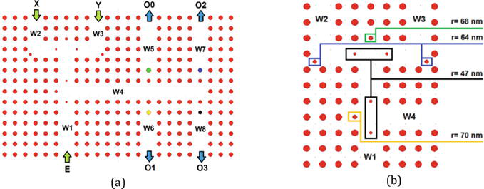
Recently, a wide range of optical decoders has been designed based on nonlinear cavities. The amount of their contrast ratio, time analysis, and area distinguishes them from each other. There is a report of a 2-to-4 decoder which is constructed by eight waveguides, which are connecting two input ports, X and Y to four output ports, O0, O1, O2, and O3 (see Figure 3a) [7]. One bias signal from port E is applied to the waveguide W1 for interfering with two signals coming from input ports through the waveguides W2 and W3. Four nonlinear rods made of doped glass with a linear refractive index and a nonlinear coefficient are placed in waveguides W5, W6, W7, and W8.
Figure 3.
(a) A top view of the structure including four resonant cavities connected to W5, W6, W7, and W8 [7] (b) magnifying the cross-connection for inputs X and Y [7].
Due to the optical Kerr effect, the value of the refractive index for a dielectric material depends on the applied optical intensity. Using the different radii in the cavities, in addition to the optical Kerr effect, makes the dropping operations for the different intensities through the cavities. By changing the values of radii for nonlinear rods with a step of 1 nm and calculation of the power at output ports, the radii of 118, 111, 104, and 97 nm were assumed for rods with green, yellow, blue, and black colors in waveguides W5, W6, W7, and W8, respectively. So, the different optical intensities in waveguide W4 in response to the different states of the input ports will be dropped through waveguides W5, W6, W7, and W8 for achieving the decoding operation. The radii of some rods in waveguides W1, W2, and W3 have been given in Figure 3b. In the corners of waveguides W2 and W3, two rods with radii of 64 nm have been placed to increase the transmission of optical waves at the bends. Four rods with radii of 74 nm, in addition to one rod with a radius of 70 nm, are considered in waveguides W1, W2, and W3 for approaching the desired interferences at the cross-connections of the waveguides. So, the different optical intensities in waveguide W4 in response to the different states of the input ports will be dropped through waveguides W5, W6, W7, and W8 for achieving the decoding operation. The consumption power is 10 mW/μm2. Also, the delay time of the proposed structure was obtained around 220 fs, in the area of 90 μm2. Furthermore, the difference in the margins for logic 0 and 1 was calculated at around 83%.
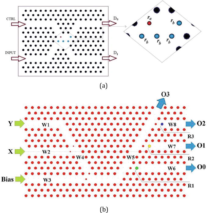
In the other article [8], a photonic crystal-based structure has been proposed for the all-optical 2-to-4 decoder. The structure consists of an array of 19 × 15 chalcogenide rods in the form of a square lattice, which consists of two input ports X and Y, one bias signal E, and eight waveguides (named W1, W2, W3, W4, W5, W6, W7, and W8) for transmission of input waves toward the output ports O0, O1, O2, and O3 (see Figure 4a). A bias and two input signals are guided through the three waveguides toward the cross-connections to have constructive interferences. The obtained signal is transmitted through a waveguide that is connected to three nonlinear cavities. To approach the optical Kerr effect, one rod made of a doped glass is placed in each cavity. Based on the amount of the optical intensity, as shown in Figure 4b, the maximum normalized powers at ports O0, O1, and O2 approximately occur for intensity of I0, 2I0, and 3I0, respectively, the waves are dropped and guided toward the desired output ports. The footprint of the device is 76 μm2. Furthermore, the delay time of the proposed structure is approximately equal to 210 fs. Besides, the contrast ratio of output ports has been obtained at 13.52 dB.
Figure 4.
(a) A 2-to-4 decoder with three cavities [8] (b) normalized power for coupling in cavities versus the optical intensity in W1 [8].
Unlike the two previous decoders with square lattice [7, 8], the two following decoders [9, 10] present a triangular lattice of the two-dimensional photonic crystal in the design of an all-optical decoder based on cavities (see Figure 5). To control and conduct light, linear and point defects are developed in curved directions. In addition to the main entrance, a controlling entrance was assumed to control light using light interference theory when the input source is active and to activate the intended output in its absence. Figure 5a shows a 1-to-2 decoder that has an upper defect with a hexagonal cavity [9]. When the input is zero, light reaches the boundary of the two waveguides from the optical source is intensified through the cavity, and is conducted in the D0 direction. The cavity acts as a resonator and can amplify the light before it reaches D0 output. If the input is “1”, the light from this source affects the control source light and prohibits it from reaching the light in the cavity. The light of the control source, thus, is not able to transmit to the D0 output. In addition, the input source light plus some other sources transfer to the D1 output. The results show that the structure can be used as a decoder with a bit rate of about 2Tbit/s and a time delay of 0.1 ps. The contrast ratio is 84%.
Figure 5.
(a) Some defects at the center of cross-connection for approaching decoding operation [9] (b) cavity connection to a main waveguide with nonlinear rods for decoding [10].
As shown in Figure 5b, the proposed structure [10] consists of two input ports (X, Y), and one bias port Z to apply the incoming optical signals. Four waveguides (W1, W2, W3, and W4) transmit the optical waves to the W5 waveguide. To prevent backward waves, four defects are placed at the cross-connection of W4 with W2 and W3. With respect to the amount of optical intensity inside W5, three nonlinear cavities drop the waves toward O0, O1, and O2 output ports through W6, W7, and W8 waveguides, respectively. If the dropping operation is not done by the mentioned cavities, the waves reach the O3 output port. Three nonlinear rods made of doped glass are placed in the cavities. The time analysis of the device shows the rise time is equal to 200 fs. The area of 110 μm2 and the margins of 4 and 88% for logics 0 and 1.
4.2 Ring-based structures
The other group of all-optical decoders based on photonic crystals is the ones that are designed with the help of ring resonators. That is to say, rings play an important role in conducting or filtering incoming light toward output ports by use of nonlinear defects. In this section, three structures are investigated and all of them are based on rings. First of all, it is worth mentioning that all rings cannot be activated when the two input ports connected to the rings are active. That is why the refractive index of nonlinear defects is placed around rings by increasing incoming power changes. As a result, the wavelength of rings alters, and the light is not able to circulate through the ring.
In Ref. [11], a 2-to-4 decoder composed of six rings has been introduced. One bias signal is needed to perform as enabling port. This port is called the bias port. The schematic of the proposed structure is shown in Figure 6. There are two input ports labeled as port A and port B and also four output ports named O1, O2, O3, and O4. Six rings are highlighted and labeled as ring #1 to ring #6. Depending on input intensity through ports A and B, impelled pulse through the bias port will be guided through ring resonators and each of the output ports will be on. The proposed structure for the optical decoder is suitable for compact integrated circuits due to its total size of 512 μm2. Power analysis has shown that power levels for logic 0 and 1 are 0.1Pin and 0.37Pin (Pin is input power), respectively. Since the maximum response time of the decoder is about 6 ps, the operation speed will be more than 160 GHz which makes it appropriate for being a part of ultrafast optical communication systems. The insertion loss of the decoder is between −2.76 and −20 dB and cross talk is between −15.6 and −38 dB.
Figure 6.
Designing a 2-to-4 decoder using six-ring resonators [11].
It can be inferred that the needed input intensity for activating rings depends on the nonlinear coefficient of the ring resonator. In the two next decoders [12, 13], chalcogenide glass is used instead of silicon because of the higher nonlinear refractive index. The most important advantage of using this ring is its nonlinear coefficient. According to the Kerr effect, the greater the nonlinear coefficient, the lower the input intensity needed for switching applications.
As shown in Figure 7, the all-optical 2-to-4 decoder [12] based on photonic crystal nonlinear ring resonators has one enable port (port E) which can control decoding operation. Also, four ring resonators are used, two input ports labeled as the port X and Y and four output ports named O0, O1, O2, and O3.
Figure 7.
Using four rings including nonlinear rods for decoding two inputs X and Y [12].
In order to reduce the input power intensity, nanocrystal rings, which have a high Kerr coefficient, are placed in the center of all-optical switches. Thus, the required optical intensity was reduced to 13 mW/μm2. The operation speed of the decoder is about 160 GHz. The worst output power levels for logics 0 and 1 are 0.1Pin and 0.63Pin, respectively. The maximum insertion loss is −4.31 dB, and the maximum calculated cross-talk is −17.53 dB. Since the total size of the structure is 368 μm2, it can be a suitable candidate for compact optical circuits.
Figure 8 shows a 2-to-4 all-optical decoder based on three resonant rings [13]. In fact, this device could be considered an improvement of the structure shown in Figure 7. The maximum response time and the switching speed are 2 ps and 500 GHz, respectively, better than those in the previously mentioned works [12]. In addition, the size of the proposed decoder is 380 μm2. The power level margins for logic states 0 and 1 are equal to 0.14 Pin and 0.49 Pin, respectively.
Figure 8.
Decoding of two bits using three resonant rings [13].
By realizing the two mentioned types of resonators, a design for an all-optical 2-to-4 decoder has been proposed [14]. The structure consists of one nonlinear ring and three nonlinear cavities that have been modified for entering the slow-light regime to enhance coupling through waveguides (see Figure 9). More coupling in waveguides resulted in more power at output ports. So, the margin of the high level was increased from 82 to 99% for output ports, which is more than in other works [7, 8, 9, 10, 11, 12, 13, 14]. Also, the size of the device is 228 μm2 more compact than some works [12, 13].
Figure 9.
Using resonant cavity and ring for designing a 2-to-4 decoder [14].
The structures based on cavities generally have smaller sizes than that of the ones based on rings. The important parameters of the mentioned works are summarized in Table 2. It can be seen that references [7, 8, 9, 10] which are based on cavities have smaller sizes than references [11, 12, 13, 14], which are designed by resonant rings. According to the published works and Table 2, it is recommended a lattice form and a cavity-based resonator to design the photonic crystal decoders with fast response and small area. If transmission efficiency is the main parameter to design the photonic crystal, ring-based decoders are the first choice. Due to the compatibility with the fabrication technologies, silicon and chalcogenide are the relevant materials in the design of the photonic crystal decoders. The possibility of high doping in chalcogenide and high optical Kerr coefficient makes it an excellent material for nonlinear rods into the resonators.
This chapter considers different ideas and designed structures for photonic crystal-based decoders. In the first section, the importance of the optical devices and the main challenges in light confinement and designing proper waveguides are investigated. Then, the excellent features of photonic crystals for the realization of decoders are presented. In Section 2, the decoder as a digital device is introduced and its truth table is given. Photonic crystals are discussed as a medium for transmission and manipulating optical signals, in Section 3. Moreover, the main parameters of these crystals are introduced. In Section 4, a strategy for designing the photonic crystal-based decoders has been introduced and some recommendations are given. Concerning the raised strategy, different decoders are categorized into cavity-base and ring-base structures. Also, a comparison of these works including lattice form, material, contrast ratio, size, and time response has been presented. The comparative view makes a vision to researchers for future works in designing photonic crystal decoders.
1.Maleki MJ, Soroosh M, Akbarizadeh G. A subwavelength graphene surface plasmon polariton-based decoder. Diamond and Related Materials. 2023;134:109780. DOI: 10.1016/j.diamond.2023.109780
2.Morris, Mano M, Ciletti M. Digital Design: With an Introduction to the Verilog HDL, VHDL, and System Verilog. 6th ed. India: Pearson; 2017
3.Joannopoulos JD, Meade RD, Johnson SG, Joshua N. Photonic Crystals: Molding the Flow of Light. 2nd ed. USA: Kindle; 2011
5.Robinson S, Nakkeer R. Photonic Crystal Ring Resonator Based Optical Filters. London, UK: InTech; 2013. DOI: 10.5772/54533
6.Prather DW, Sharkawy A, Shi S, Murakowski J, Schneider G. Photonic Crystals, Theory, Applications and Fabrication. 1st ed. USA: Wiley; 2009
7.Maleki MJ, Soroosh M, Mir A. Improving the performance of 2-To-4 optical decoders based on photonic crystal structures. Crystals. 2019;635:1-9. DOI: 10.3390/cryst9120635
8.Maleki MJ, Soroosh M. A novel proposal for performance improvement in two-dimensional photonic crystal-based 2-to-4 decoders. Laser Physics. 2020;30:076203-076209. DOI: 10.1088/1555-6611/ab9089
9.Parandin F, Karkhanehchi MM, Naseri M, Zahedi AH. Design of a high bitrate optical decoder based on photonic crystals. Journal of Computational Electronics. 2018;17:830-836. DOI: 10.1007/s10825-018-1147-3
10.Maleki MJ, Soroosh M, Mir A. Ultra-fast all-optical 2-to-4 decoder based on a photonic crystal structure. Applied Optics. 2020;59:5422-5428. DOI: 10.1364/AO.392933
11.Daghooghi T, Soroosh M, Ansari-Asl K. A novel proposal for all-optical decoder based on photonic crystals. Photonic Network Communications. 2018;35:335-341. DOI: 10.1007/s11107-017-0746-4
12.Daghooghi T, Soroosh M, Ansari-Asl K. A low-power all optical decoder based on photonic crystal nonlinear ring resonators. Optik. 2018;174:400-408. DOI: 10.1016/j.ijleo.2018.08.090
13.Daghooghi T, Soroosh M, Ansari-Asl K. Ultra-fast all-optical decoder based on nonlinear photonic crystal ring resonators. Applied Optics. 2018;57:2250-2257. DOI: 10.1364/AO.57.002250
14.Daghooghi T, Soroosh M, Ansari-Asl K. Slow light in ultracompact photonic crystal decoder. Applied Optics. 2019;58:2050-2057. DOI: 10.1364/AO.58.002050
Written By
Mohammad Javad Maleki, Mohammad Soroosh, Fariborz Parandin and Fatemeh Haddadan
Submitted: 05 July 2023Reviewed: 09 July 2023Published: 06 October 2023
 Open access peer-reviewed chapter