 Open access peer-reviewed chapter
Abstract
The recent developments of optoelectronics do promote the progress in many other fields. For quantum information processing, we made efforts in manufacturing quantum devices by using optoelectronic techniques. We designed quantum dot embedded nanocavities to serve as efficient quantum emitters; using spectral multiplexing technique, we fabricated a heralded single-photon source, emitting highly pure and speedy single photons; and defects in GaN were observed serving as room temperature quantum random number generators. An entangled photon emitter with visibility of 97% was developed using cascaded second-order nonlinear optical process in PPLN waveguides; and Si3N4 microrings were effectively applied to establish photon entanglers. Readout circuits were optimized to fabricate specific single-photon avalanche detectors, and telecomm-band single-photon avalanche detectors have been improved to 128 × 32 arrays for quantum imaging. A multiplexed quantum memory was explored to simultaneously store 1650 single photons. Opto-electro-mechanical devices were studied or fabricated in order to measure minor quantities in quantum level. These works may shed light on quantum information technology for the future.
Keywords
- optoelectronics
- device
- quantum information
- single photon
- entanglement
1. Introduction
Quantum information science has now attracted significant attention, since it has been well proved and is believed to support quantum computation, quantum communication, and quantum metrology in the near future by using unique quantum mechanical characteristics [1]. Characteristics of quantum states have opened the opportunities to accomplish tasks beyond classical limits, resulting in a frontier field of quantum technologies [2, 3, 4, 5, 6, 7, 8]. Among them, quantum computation technology can accelerate the speed of computers exponentially with respect to the classical machine, quantum communication technology guarantees completely secure communication [9, 10, 11, 12, 13, 14], and quantum measurement technology can greatly optimize the sensitivity and/or resolution of many instruments [15, 16, 17, 18]. These potential accomplishments have led to the development of innovative and advanced applications in various sectors such as the military, communication, and therefore, people are presently struggling to construct efficient quantum information systems and quantum networks [10, 19, 20, 21, 22, 23].
To realize practical quantum information systems and quantum networks, fundamental devices must be firstly well developed. The successful fabrication of superconductor quantum circuit chips led to an achievement of constructing quantum computer of 127 qubits [24]. Realization of more general quantum computers needs much larger scaled, more robust, more quantum logic circuit chip consisting of probably superconductors [25], cold atoms [26], semiconductors [27], photonic crystals [28], etc. The primary obstacles in establishing a quantum network involve the distribution of entangled qubits among nodes that are physically distant from each other, which need high-performance entangled photon source and quantum memory [29]. Among various types of quantum devices, optoelectronic devices play a key and central role, since the advanced microelectronic, optical, and optoelectronic platforms enable fabricating the building blocks for most of the quantum information processing systems [30]. Technologies based on optoelectronics have the potential to realize a complete product chain in the field of quantum information [31, 32].
Materials with optoelectronic properties for quantum information applications encompass crystals exhibiting optical nonlinearity [33], semiconductors with wideband characteristics [34], semiconductor quantum dots [35], optical fibers, photonic crystals, diamonds, 2D materials [36], perovskites [37], metamaterials [38], topologic insulators, etc. These materials have been utilized in the development of various quantum devices such as circuits, emitters, detectors, memories, repeaters, channels [33, 34, 35, 36, 37, 38], but further developments are still strongly required, for example, to improve the scalability of quantum information networks. To face up with the coming challenges, we need first look back what we have really resolved and probably see how we can step forward.
In this chapter, the optoelectronic devices we manufactured for quantum information processing will be reviewed. Our works on single-photon emitters, entangled photon sources, single-photon detectors, and other devices will be described in sections 2, 3, 4, and 5, respectively. At the same time, we also discuss some demonstrations and applications using these devices. We hope this review is helpful for the realization of quantum information network in the future.
2. Single-photon emitters
Single-photon emitters refer to light sources that release light in the form of individual particles or photons. Single-photon emitters are the fundamental devices for quantum communication. They are also well used in quantum detection and photonic quantum computation. In this direction, we have studied single-photon emitters based on quantum dot [32, 39, 40, 41, 42], heralded single-photon sources [43], identity of single photon [44], and a quantum random number generator [45].
2.1 Quantum dot single-photon emitters
Most of the single-photon emitters in use are probabilistic devices [46], which are not well satisfying the sophisticated requirements of quantum information system. Semiconductor quantum dots (QDs) are tiny particles, typically a few nanometers in size, which exhibit distinct optical and electronic characteristics due to the principles of quantum mechanics. QDs are believed to be ideal candidate for on-demand, deterministic single photon emitters, so materials containing QDs were deeply investigated to pursue quantum emitters based on QDs, for which we have a review paper [47]. Early in 2005, we participated in the work from Ref. [43], where remarkable photon antibunching was obtained from the InAlAs single QD, and its further strengthened single-photon generation was demonstrated [39]. These devices were designed to match the visible light range of the highly efficient Si single-photon detectors, but higher requirements lie in the telecommunication bands. For the application in optical fiber-based quantum communication, we have fabricated InAs/InP quantum dot single-photon emitter and achieved the highest single-photon purity (~10−3) [40]. This source has been applied in a conventional system of quantum key distribution and effectively practiced secure key transmitting over 50 km of commercial fiber. These single photo-emitters, however, were subject to low-emitting rates, which is hindering its application in quantum communication. Using the cavity Purcell effect to modulate the QD lifetime, we designed Si/SiO2 distributed Bragg reflectors (DBR)-based micropillar cavities in hybrid with InP-based semiconductors for weak [48] and strong coupling (with tapered DBR) [49] of telecom-band photons with QDs to achieve highly efficient, indistinguishable, and even coherent single-photon emitters.
Considering the difficulty in hybrid processing, we then designed monolithic micropillar InP-based single-photon emitters [41, 50, 51]. In these works, new designs for pillar cavities operating at a wavelength of 1.55 μm were proposed and investigated. These structures consist of layers made from InP, air apertures, and InGaAsP materials. It has been verified that these structures can be manufactured using a single-integrated process. By incorporating air apertures and tapered DBRs, it is possible to achieve a high-quality factor ranging from 104 to 105 at the desired wavelength of 1.55 μm.
The diagram of the proposed cavity is schematically demonstrated in Figure 1(a). Figure 1(b) displays the instances of the computed optical mode spectra accompanied by corresponding DBR optical bands. This nanocavity exhibits potential as a promising option for QD single-photon sources in the 1.55-μm telecom band, owing to its capability to achieve both weak coupling and strong coupling between a single semiconductor QD and an optical cavity mode. The above cavity design using adiabatic tapering technique was later extended to a general method, by which one can realize different types of highly efficient quantum emitters [52, 53].
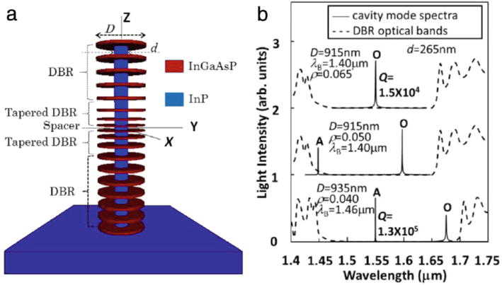
Figure 1.
(a) A visual representation of the proposed cavity in three dimensions. (b) Optical mode spectra and corresponding DBR optical bands were calculated, with vertical shifts applied to lines representing different design conditions for clarity. From ref. [
Based on these proposals, we further studied their possible advancements to achieve high experimental availability [42, 54]. The impact of fabrication tolerance on the InGaAsP/InP-air-aperture micro−/nano-pillar cavity was investigated in our work. A finite-difference time-domain method was employed to simulate the effects of fabrication imperfections, encompassing uncertainties in layer thickness, material diameter, surface and interface roughness, and distortion of the cavity shape. The results indicated the cavity quality was robust to the imperfection of the fabrication processing. The cavity quality remained sufficiently high to create highly efficient and coherent single-photon sources at a wavelength of 1.55 μm, even with thickness errors within the range of ±2 nm, diameter uncertainties within ±2%, surface roughness variations up to ±2.5 nm, and sidewall inclinations of 0.5°. Consequently, an InGaAsP/InP-air-aperture micropillar cavity containing quantum dots shows promising potential as a realizable choice for single-photon emitters in quantum information networks based on silica fibers.
2.2 Heralded single-photon source
The above QD single-photon emitters are currently not practical enough yet, so people have to seek more useful candidates for on-demand single-photon emission. Heralded single-photon source (HSPS) represents such efforts. Although still probabilistic, it can partially approach the deterministic character. It is based on correlated photon pairs, in which one photon (the heralding photon) is detected and the existence of the other photon (the heralded photon) can be indicated. The generation of correlated photon pairs can be realized through the processes of spontaneous parametric down-conversion (SPDC) or spontaneous four-wave mixing. Besides the nearly deterministic property, such HSPSs have the advantages of convenient demonstration, flexible emission wavelength, and high indistinguishability. Lithium niobate is the most advanced material for optoelectronic and optical quantum devices, for which we have a review paper [55]. In Ref. [43], we have proposed a 1.5 μm chip-scale HSPS made of lithium niobate on insulator (LNOI) by utilizing spectrum multiplexing and active feedforward spectrum processing technology, as shown in Figure 2.
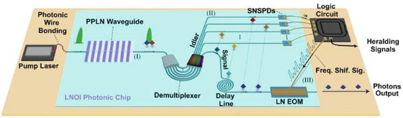
Figure 2.
A view on the future chip-scale spectrally multiplexed HSPS using LNOI technology, where a single photonic chip integrates all essential components including modules of a pump laser, a photon-pairs generator, a filter and detector, and a feedforward and frequency shifter. From ref. [
Furthermore, we have successfully demonstrated a preliminary experiment using discrete fiber-based elements, as depicted in Figure 3. The broadband correlated photon pairs were generated within a fiber-connected periodically polarized lithium niobate (PPLN) waveguide. Next, the dense wavelength-division multiplexers (DWDMs) were utilized to segregate the signal photons and heralding photons, which had a bandwidth of approximately 100 GHz. The heralding photons from three paths were individually detected by three superconductor nanowire single-photon detectors (SNSPDs).
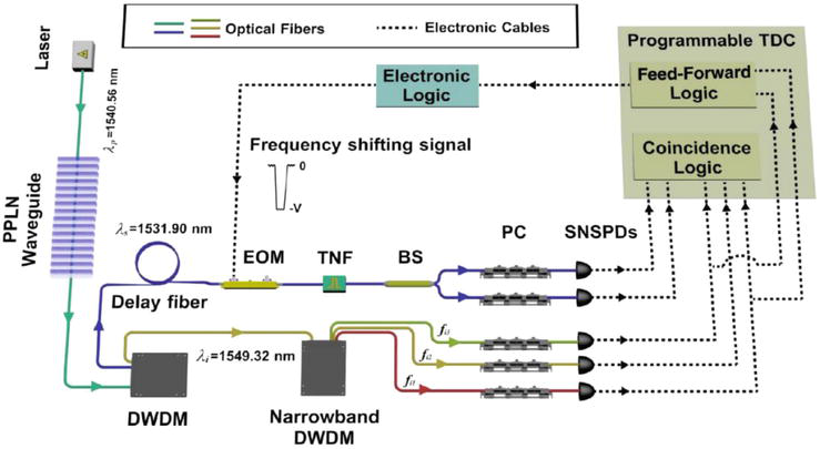
Figure 3.
Experimental setup for spectrally multiplexed HSPS. From ref. [
As a result, the detecting events of those photons were directed to the feedforward logic where every detecting event activates the logic circuit, causing electronic devices emit an associated frequency-shifting signal to the electro-optical modulator (EOM). The signal photons underwent a delay through a fiber loop in order to synchronize their timing with the electronic frequency shifting signal. Subsequently, the signal photons experienced frequency shifting and were combined into a shared spectral mode. Ultimately, an exceptionally low second-order correlation index g2(0) of 0.0006 ± 0.0001 was achieved at a tested single-photon emitting rate of 3.1 kHz, indicating that spectral multiplexing has enhanced the heralded single-photon rate by nearly threefold. Moreover, by implementing Hong–Ou–Mandel (HOM) interference between these spectra-multiplexing single photons and photons from independent and weakly coherent sources, it was demonstrated that the indistinguishability of multiplexed single photons after spectrum manipulation is ensured. This research opens up possibilities for scalable and highly performing HSPS on-chip with spectral multiplexing toward deterministic single-photon emitters.
2.3 The identity of single photons
For quantum information processing, for example, quantum teleportation and quantum key distribution, the issue of indistinguishability between wave packets of individual photons has been emphasized. At present, the indistinguishability of single photons has been characterized from different perspectives, such as space, time, polarization, frequency, and orbital angular momentum. From Ref. [44], we have specifically studied the evolution law of photon identity from the perspective of dispersion through the HOM interference. In this work, a theoretical analysis model of photon identity from the perspective of dispersion was established based on HOM interference. We initially generated two wave packets with weakly coherent single photons by attenuating pulses from a mode-locked laser and subsequently manipulated them in a dispersive manner prior to their interference. The outcome demonstrated that the second-order dispersion related disparity between the two optical paths of the HOM interferometer can be correlated with the interference pattern. When both paths experienced an equal amount of dispersion, the pattern was determined by the inherent indistinguishability of the wave packets. Conversely, if there was an imbalance in dispersion between the paths, it would broaden the interference pattern and diminish its visibility. This study offers a more comprehensive comprehension of single-photon wave packets and explores potential applications of HOM interference in quantum information processing based on single photons.
2.4 Application: Quantum random number generator
Random numbers have a widely application in field of quantum information processing. Among the different types of random number generators, quantum random number generators (QRNGs) can generate true and unpredictable random numbers by utilizing inherent randomness in a system based on quantum mechanics.
Firstly, we have successfully demonstrated the single-photon emission at room temperature from a single defect in a GaN layer grown on a patterned sapphire substrate [45]. This emission exhibited a rate of 2 MHz and an auto-correlation value of 0.36 ± 0.01. Additionally, we have conducted an experimental validation of a real-time quantum random number generator utilizing the aforementioned single-photon emitter, as depicted in Figure 4. The excitation of the single emitter was achieved using a continuous wave laser with a wavelength of 532 nm. By employing a dichroic mirror (DM) with its cutoff wavelength set at 560 nm, the laser beam was reflected and focused onto the GaN wafer through an objective lens with numerical aperture (NA) equal to 0.9. Subsequently, the obtained luminescence resulting from this process was collected by the objective lens as above configured in confocal mode before being directed toward our detection system
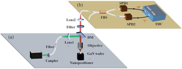
Figure 4.
Scheme of a random bit generator with branching paths. (a) the experimental setup, which involved a self-made confocal scanning microscope to stimulate the single-photon emission in the GaN wafer and capture the luminescence from individual photons. (b) the HBT configuration, employed to assess the purity of single photons emitted and generate binary random numbers. From ref. [
3. Entangled photon sources
Quantum entanglement is a phenomenon that arises when a collection of particles is created, interact, or exist in close proximity to each other in such a manner that the individual quantum states of each particle cannot be figured out independently from the states of the others, even if these particles are widely separated. As a fundamental resource, quantum entangled light sources are widely used in quantum information processing [56, 57, 58]. We have made a comprehensive study on the theory [59], performance improvement [60, 61], integration [62, 63], and application [64, 65, 66] of entangled photon sources.
3.1 Theoretical study on entangled photon sources
Entangled photons with a wider wavelength range are conducive to expanding their application scenarios in quantum information processing. However, typical materials for the preparation of spectrally uncorrelated entangled photon pairs are limited to a few nonlinear crystals, making the range of photon wavelengths not as wide as ideal. To explore new schemes for obtaining a wider wavelength range, we have theoretically studied the spectrally uncorrelated entangled photon pairs produced by 15 isomorphs of potassium dihydrogen phosphate (KDP) crystal [59]. The results show that eight crystals in the “KDP family” have nonlinear optical properties similar to KDP and have the ability to generate spectrally uncorrelated entangled photon pairs within a wavelength range of ~300 nm (i.e., 792 ~ 1092 nm) according to the group velocity matching condition. Furthermore, we have investigated the preparation of heralded pure-state single photon with a purity of 0.97; namely, the output of one single photon was herald from the detection signal of another photon in the photon pair. The HOM interference between photons from independent emitters also achieved a visibility around 97%. The work expands the preparation of entangled photon pairs as well as heralded pure-state single photons with a wider wavelength range in the near-infrared band.
3.2 Performance improvement of entangled photon sources
Acting as information carriers, photons can be entangled in various degrees of freedom, such as polarization, frequency-bin, time-energy, orbital angular momentum, time-bin. To obtain high-performance discrete frequency-bin entangled photon pairs, we have proposed and demonstrated a scheme consisting of a modified Sagnac interferometer by using a single piece of PPLN waveguide [60]. The correlated two-photon states were prepared in different directions of a Sagnac interferometer based on cascaded SHG/SPDC processes. The output two-photon states could be manipulated by introducing the relative phase difference between two transmission paths with the change of polarization state of pump laser. Then, the discrete frequency-bin entangled photon pairs were obtained by using a fiber polarization splitter without post-selection. The performance of frequency-bin entangled photon-pairs is shown in Figure 5. The prepared frequency-bin entanglement achieved a fidelity of 98.0 ± 3.0% based on the visibility of spatial quantum beating of 96.0 ± 6.1%. It provides a practical frequency entangled photon source compatible with the modern telecommunication for quantum information processing.
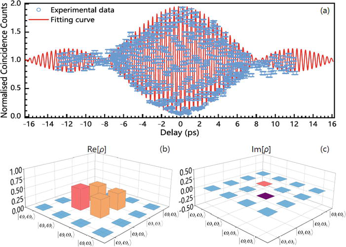
Figure 5.
The photon pair performance of frequency-bin entangled sources. (a) the spatial quantum beating; (b) the real part; and (c) the imaginary part of the density matrices, respectively. From ref. [
The practicality of entangled photon sources limits their application in quantum information processing. To obtain entangled photon pairs with high performance, we have proposed a scheme of fiber-integrated PPLN waveguide module that consists of a PPLN waveguide and two noise-rejecting filters [61]. Figure 6 shows the structure of the module and the measured spectra of correlated photon pairs and Raman photons from the module. The correlated photon pairs were prepared by cascade SHG/SPDC processes in a PPLN waveguide of a single piece. As a result, the coincidence-to-accidental ratio (CAR) of photon pairs achieved a maximum value of 52,600, and the generation rate and detection rate were 52.36 kHz and 3.51 kHz, respectively. It was actually improved for nearly one order of magnitude with respect to the previous reports.
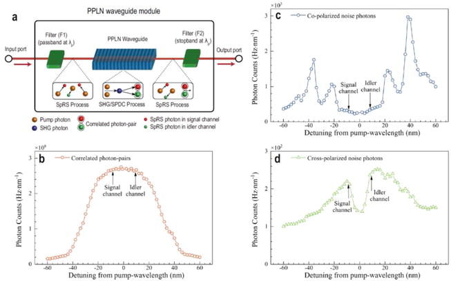
Figure 6.
(a) The structure of the PPLN waveguide module. (b) the spectra of correlated photon pairs generated from the module. (c), (d) the spectra of co- and cross-polarized Raman photons from the module. From ref. [
Based on the coherently superposition of correlated photon pairs, we have further prepared energy-time, time-bin, and frequency-bin entangled photon pairs to cope with different application scenarios, respectively, as shown in Figure 7. The visibility of the two-photon interference of the energy-time entangled photon pair was 95.74 ± 0.86%, and the maximum S = 2.71 ± 0.02 of the Clauser–Horne–Shimony–Holt (CHSH)-Bell inequality could be calculated. The fidelity of the frequency-bin entangled photon pairs was measured to be 97.56 ± 1.79%, while the visibility of the spatial quantum beating reached 96.85 ± 2.46%. Quantum tomography revealed fidelity of 89.07 ± 4.35% for the time-bin entangled photon pairs. Our results provide a high-performance entangled photon source in quantum information processing, which can cope with various application scenarios.
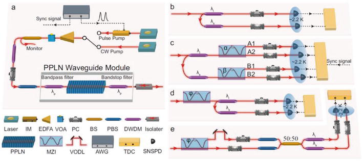
Figure 7.
Experimental setups. (a) Generation of correlated photon pairs. (b) Characterization of correlated photon pairs. (c) Characterization of energy-time and time-bin entangled photon pairs. (d) Coherently manipulation of energy-time entangled photon pairs. (e) Generation and characterization of frequency-bin entangled photon pairs. From ref. [
3.3 Efforts on chip-level entangled photon sources
As is well known, in order to realize highly-performing quantum information processing, the development of thoroughly integrated photonic chips based on various materials and schemes has become an inevitable tendency. We have investigated the generation of multi-wavelength correlated photon pairs
In addition, we have experimentally demonstrated a multi-wavelength quantum light source with a Si3N4 MRR [63]. The device design and characterization are shown in Figure 8. The optimized over-coupling Si3N4 MRR was designed and fabricated with the free spectral range around 200 GHz and the quality-factor about 1.0 × 10⁶. The generation of eight high-quality correlated photon pairs with high photon generation rate, CAR, and single-photon purity was achieved by the natural resonance characteristics. With device optimization and noise-rejecting filters, we further prepared heralded single photons and energy-time entanglement for each wavelength pair. The results show a second-order auto-correlation value of
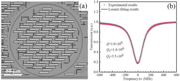
Figure 8.
Device design and characterization for Si3N4 micro-ring entangled photon source. (a) Microscopy image of the silicon nitride micro-ring with a thickness of 0.8 μm, width of 1.8 μm, radius of 113 μm, and gap width of 0.35 μm. (b) Resonance dip at 1540.5 nm, with a
3.4 Application of entangle photon sources
Based on the previous works on high-performance entangled photon pair, we have explored their application in quantum information processing including quantum teleportation [64, 65] and quantum key distribution (QKD).
Quantum teleportation is one of the methods of quantum communication, which could transfer an unknown quantum state between two remote nodes
Based on the experience of previous experiment in the lab, we have further implemented the quantum teleportation system
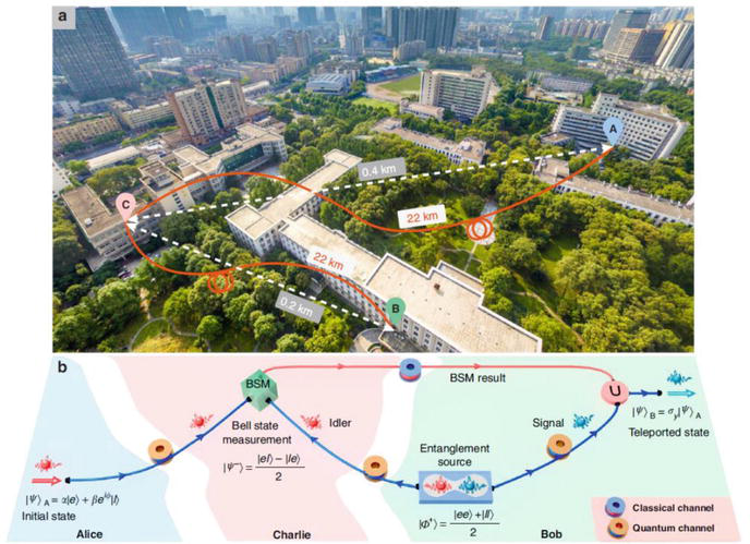
Figure 9.
(a) Aerial view of the teleportation system based on UESTC backbone network. (b) Scheme of the teleportation system. From ref. [
The characteristics of the system relied on a high-performance time-bin entangled photon source mentioned before [61]. In our system, we also have built a real-time feedback system to adjust arrival time and polarization of single photons. In this way, the indistinguishability of photons distributed through fiber channels could be guaranteed, thus achieving efficient BSM. As a consequence, we have successfully implemented a quantum teleportation system operating at a rate of 7.1 ± 0.4 Hz over a fiber channel spanning 64 km in a metropolitan area. Moreover, employing the decoy state technique, we achieved an average fidelity of single photons at approximately 90.6 ± 2.6%. This implementation marks a significant achievement in the development of quantum internet and paves the way for investigating applications of quantum information utilizing a source of entangled photons.
Quantum key distribution (QKD) establishes a private, shared cryptographic key between the remote parties. The QKD based on quantum entanglement is important for future quantum secure communication networks, because photonic entanglement could be extended over remote notes and may not require additional quantum random number generators. To date, most of works on this topic have employed dark fibers. It would be more preferable to develop quantum network coexisting with classical fiber communication system. Therefore, we have successfully demonstrated the coexistence of energy-time entanglement-based QKD and classical optical communication using DWDM in the telecom C-band [66]. The configuration is illustrated in Figure 10. Consequently, we have experimentally verified that energy-time entanglement-based QKD can coexist with bidirectional 20 Gbps data communication over a 40-km-long optical fiber. Ultimately, employing the BBM92 protocol for QKD, we achieved a raw key generation rate of 245 bits per second and a quantum bit error rate of 8.88%. This experimental demonstration highlights the convenient compatibility between entanglement-based QKD and classical fiber communication, showcasing its immense potential for quantum networks.
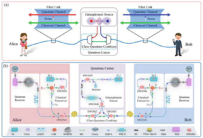
Figure 10.
(a) Illustration of entanglement distribution coexisting with classical fiber communication system. Entangled photons are distributed to Alice and bob. (b) Experimental setup in 40-km fiber [
4. Single-photon detectors
A single-photon detector is a photodetector, which can respond to incident light signal as weak as one single photon. Single-photon detectors play a widespread role in the field of quantum information processing since they serve as key devices, for example, readout in quantum computing, receiving in quantum communication and photon measurement in quantum metrology. We have had a review paper on a single-photon detector [67]. We focused our research on Geiger-mode avalanche photodiodes (single-photon avalanche diodes [68, 69], negative feedback avalanche diodes [70]) and the application of the two-dimensional (2D) materials for photon-level detectors [71]. Moreover, we have proposed fiber Bragg grating sensing system by utilizing single-photon detectors [72, 73].
4.1 Single-photon avalanche detectors
Avalanche photodiodes (APD) have been well studied and well fabricated for the application in many fields, for which we had a review paper on our previous works [74]. Geiger-mode (GM) avalanche photodiodes (APD) have detecting sensitivity as precise as single-photon level, so they are usually also termed as single-photon avalanche detectors (SPADs). Based on our previous works [69, 74], we recently performed more studies on Gm-APD or SPAD design and fabrication. In Ref. [68], we have proposed a detecting system of high-speed photon counting rates with an active quench and reset integrated circuit (AQR-IC) driving a InGaAs GM-APD at near-infrared range. The APD’s parasitic capacitance and the circuit’s input port were utilized to convert avalanche current into a voltage signal. This signal was then sent to an FPGA system for calculating counting rates, with the dead time being adjusted by the FPGA for greater flexibility in photon counting applications. The AQR-IC chip and PCB-based photon counting system are depicted in Figure 11. Fabricated using SMIC 0.18 μm CMOS technology, this proposed AQR-IC can achieve the maximum photon-counting rate as high as 15.6 MHz, with dead time tunable from 64 ns up to 163.6 μs at 20 ns of resolution—thereby enhancing single photon detection flexibility when operated in free-running mode. In addition, we recently fabricated a specific free-running InGaAs SPAD device, which has a very low dark count rate of 1.6 kHz and quite high photon counting rate of ~10 MHz. This device may be more available for quantum application than those reported so far.

Figure 11.
(a) AQR-IC chip and (b) the photon counting system on PCB. From ref. [
Besides the performance improvement in single-element SPAD devices, progress has also been made on single photon imaging, that is, focal-plane single photon detecting arrays. By epitaxially growing the precise material structure and diffusing dopants locally and accurately using metalorganic chemical vapor deposition (MOCVD), fabricating the device structure using lithography, inductive coupled plasma etching (ICP), metal deposition, etc., designing and processing the integrated readout circuit chip, performing flip-chip In-shot bonding, and TEC cooled packaging, InGaAs SPAD arrays scaled 128 × 32 were successfully formed. Figure 12 shows the measured results of photon detection efficiency (PDE) and dark count rate (DCR) for one of the fabricated arrays. It indicates an average PDE of 25% and DCR mostly lower than 9 kHz. These characteristics are as good as available for application, and we are actually trying to test their performance in some application scenes such as single-photon imaging Lidar and quantum Lidar [75].
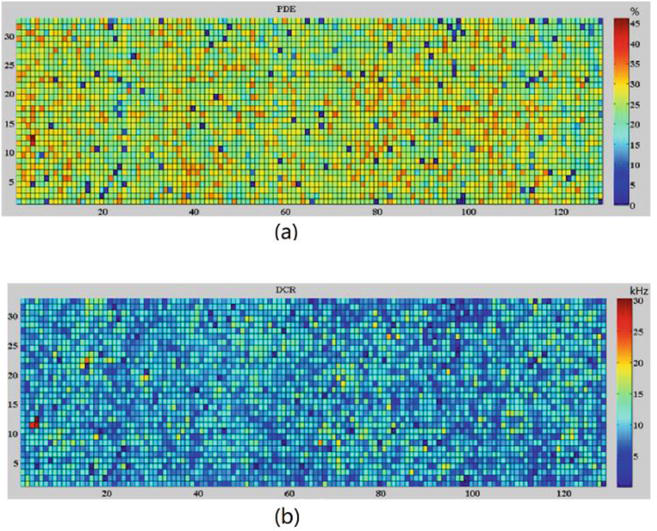
Figure 12.
The measured (a) PDE and (b) DCR of a newly fabricated 128 × 32 InGaAs SPAD array.
4.2 Negative feedback avalanche diodes for single-photon detection
With the advantages of fast quenching speed, low afterpulsing, and easy integration, negative feedback avalanche diodes (NFADs) can be used in quantum communication, fluorescence spectrum detection, single-photon counting imaging, and other application [76]. The research on NFAD devices and their application in single-photon detecting system has thus been of great significance. In Ref. [70], we have described the novel design of NFAD, and reviewed the development and application of NFAD devices in recent years. By monolithically integrating a film resistance onto SPAD, the formed self-passive quenching circuit in NFAD brings about improvements in especially afterpulsing and effectively enables photon number resolution. Further hybridizing active quenching circuit, the single-photon detection system composed of NFAD performs much better than that of conventional SPAD. Single-photon NFADs demonstrate more practical application potential in quantum information processing.
For further improvement in this field, we design new readout circuit for NFAD. To resolve the problems of avalanche signal detection and processing, afterpulsing suppression, dark counting rate, and detection efficiency of NFAD, we propose a free-running readout circuit architecture design based on InGaAs NFAD [77]. In this circuit, an ultra-low noise amplification circuit was designed, in which the noise was only ~651 μVrms. At the same time, the circuit uses digital coding to control the discrimination threshold voltage and realizes precise modulation of the threshold voltage with an accuracy of 150 μV. A control circuit module based on FPGA was then constructed. The combination of digital coding control and feedback resistance was adopted to realize a large range (4.5~90 V) and high precision (0.5%), high-voltage power output. The high precision adjustable dead time delay was realized by counting the high-frequency clock pulse signal. The photon pulse is accumulated by a 32-bit counter with high-speed (4 ns) and large-capacity counting (1 ~ 232). As a result, the minimum dead time becomes 20 ns, shorted by at least 70 ns. Finally, a single-photon counting module is built for testing the manufactured physical circuits. The results showed that the circuit can realize 0.1~100 μs dead time adjustment, and the NFAD can be much faster than before in quenching and recovering. This work provides a reference for the subsequent design of NFAD single-photon imaging system with integrated readout circuit.
4.3 Two-dimensional materials for photodetectors
The utilization of 2D substances presents a novel approach in creating nanoscale photodetectors [78]. Recent advancements have demonstrated that these 2D materials can be employed to fabricate both APDs and SPADs [79]. Our study in Ref. [80] extensively examined the structural, electronic, and optical characteristics of black phosphorus (BP) and indium selenide (InSe) monolayers, along with their BP/InSe heterojunctions using first-principle calculations. The analysis revealed that these materials possess remarkable geometric symmetry alongside appropriate bandgap values. Based on the findings regarding band offset, charge decomposition in bands, and electrostatic potential, it can be concluded that the heterojunction structure effectively suppresses the electron-hole pair recombination. This suppression is advantageous for enhancing carrier mobility in photoelectric devices. Furthermore, exceptional optical performance is observed in terms of refractive index, electron energy loss, reflectivity, absorption coefficient, extinction coefficient, and photon optical conductivity. The above outcomes suggest a promising future application potential for 2D materials in avalanche diodes or even single-photon detectors.
4.4 Application of single-photon detectors
Due to its compact size, ability to sense multiple points simultaneously, and resistance to electromagnetic interference, the optical fiber sensor that utilizes fiber Bragg gratings (FBG) is well-suited for monitoring physical variables in challenging environments including extreme temperatures [81], high pressures [82], and intense radiation [83]. By employing single-photon detectors, the FBG sensor has the potential to achieve quantum-level measurements. In a previous study [72], we have successfully demonstrated a highly efficient FBG sensing system with dense temporal multiplexing using single photon detection at 1.5-μm wavelength. A spatial accuracy of 5.0 cm has been accomplished, mainly depending on the time jitter of a single-photon detector and the duration of laser pulses. By employing the dual-wavelength differential detection (DWDD) technique, we achieved a wavelength precision of 0.5 pm within a range of 550 pm, resulting in an associated temperature sensitivity of 0.05°C. This sensitivity can be further enhanced to 0.01°C by elevating the repetition rate of laser pulses.
However, a shorter probe pulse width reaches a higher spatial resolution, which inevitably causes a spectrum broadening according to the Fourier transform theory. Namely, high-precision FBG sensing in the time and spectrum domains cannot be performed simultaneously. In Ref. [73], we have investigated the effect of spectrum broadening on a photon-counting FBG sensing system with a DWDD method. We built a theoretical model and characterized the photon-counting FBG sensing systems at different spatial resolutions. Figure 13 shows the experimental setup of high spatial resolution DWDD. A broadband coherent probe laser was generated from a mode-locked pulsed laser, and then divided into two parts by an optical coupler (OC, 90:10). One was received by an InGaAs photoelectric detector to generate a synchronizing electronic signal for a high-resolution time-to-digital converter (TDC). Then, another probe light was injected in a tunable filter to generate a pulse light with different spectral width at the central wavelength of 1550.1 nm or 1550.2 nm in turn. In order to avoid the saturation of a single-photon detector, the mean photon number of the probe laser was attenuated to 0.003 per pulse by adjusting a variable optical attenuator (VOA). As a result, a commercial FBG with a spectral width of 0.6 nm, an optimal spatial resolution of 3 mm and a corresponding sensitivity of 2.03 nm−1 can be achieved.
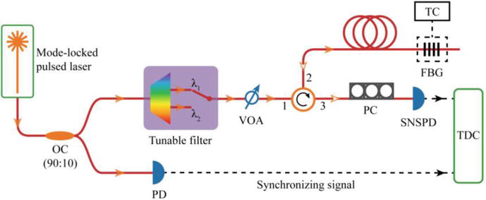
Figure 13.
Experimental setup of high spatial resolution DWDD. From ref. [
5. Other devices
In addition to the optoelectronic devices described above, we have also conducted abundant research on quantum memory [13, 84, 85], optomechanical system [86, 87, 88], and nano-opto-electro-mechanical system [89, 90, 91], including experimental studies and topic reviews.
5.1 Quantum memory
Quantum networks will probably be the main working platforms of the future quantum information technology and thus is very important in current quantum information science. Quantum memory, which is at the core of long-distance quantum repeater architectures, is the key element for quantum networks. Quantum memories have the capability to retain the quantum state of a photon or any other entangled particle while preserving its quantum information intact. In this field, we have studied photonic quantum memory based on rare-earth ions doped in solid-state materials. Erbium-doped optical fibers, which involve the incorporation of rare-earth ions into solid-state materials, exhibit efficient interaction between photons and atoms in the telecom-C band. These fibers are considered prospective candidates for quantum information processing applications, particularly in photonic quantum memory. In an experimental setting at temperatures below 10 mK, we successfully observed optical nutation in a 9.5-meter-long fiber doped with erbium ions at a concentration of 200 ppm [84]. The coherent interaction between the laser and ensemble of erbium ions resulted in the reduction of optical nutation and provided valuable insights into transition dipole moments. We investigated how transition dipole moments vary with laser wavelength and magnetic strength, finding that a transition dipole moment about 3.4 × 10⁻³² Cm was achieved at 1537 nm and 0.2 T. This research lays the foundation for realizing quantum networks in the solid-state form and operating within the telecom-C band frequency range.
Furthermore, we have demonstrated both high-bandwidth and multiplexed quantum memory for C-band photons by utilizing the atomic frequency comb (AFC) quantum memory protocol in erbium-doped silica-fiber (EDF) [85]. Figure 14 shows the experimental setup in this demonstration. The main advantage of this protocol is that the number of photons that can be stored at the same time is determined only by the time-bandwidth product. However, due to the significant inhomogeneous broadening and limited homogeneous linewidth exhibited by the employed EDF, the demonstrated quantum memory has a large storage bandwidth and a long storage time. There could be more than five spectral modes multiplexed—each 10 GHz wide—as well as over up to 330 temporal modes. As a result, we achieved the highest demonstrated multimode capacity to date, namely the simultaneous storage of 1650 heralded single photons. By making some improvements to our experimental scheme, a maximum major-mode capacity of 11,500 modes yielded by the time bandwidth product of this quantum memory could be attained. This work provides important guidance for the implementation of quantum networks based on multiplexed and broadband solid-state quantum memories.
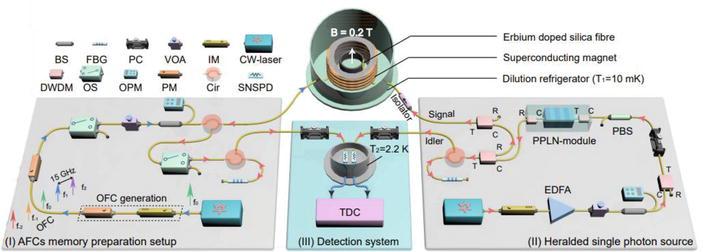
Figure 14.
The experimental setup consists of (I) multi-channel AFCs, (II) full telecom C-band heralded single photon source, and (III) measurement system. From ref. [
As described above, we have made numerous significant advances in quantum networks, including quantum photon source, quantum teleportation, quantum key distribution, quantum memory, etc.
To provide a clear understanding of the current progress and future direction of quantum networks, we conducted an analysis on the significant advancements in both theory and experimentation over the last 20 years toward establishing entangled quantum nodes and ultimately constructing a global quantum network [13]. This comprehensive review encompasses the achievements made in various physical frames including single atoms, trapped ions, cold atomic ensembles, solid-state hosts doped with rare-earth ions and diamonds with nitrogen-vacancy centers. Additionally, we explored the available methods and encountered challenges associated with building practical quantum networks.
5.2 Optomechanical system
A novel nanostructure called an optomechanical crystal nanobeam cavity has been developed, which combines both optical cavity and mechanical resonator. This innovative structure shows great potential in various applications such as modulators, sensors, and transducers. In our research, we have conducted a theoretical analysis on the impact of fabrication imperfections on the characteristics of nanobeam cavities [86]. Our findings indicate that altering the size of air holes leads to an increase in both the optomechanical coupling parameter and the optical resonance frequency, with coefficients of 0.01 MHz/nm and 0.36 THz/nm, respectively. Conversely, changing the size of air holes results in a decrease in mechanical resonance frequency at a coefficient of −0.03 GHz/nm. Interestingly, shifting the air hole line does not significantly affect any of these investigated characteristics. These insights provide valuable guidance for improving the fabrication process involved in creating nanobeam cavities.
After decades of research on entanglement generation, various schemes based on different physical platforms and information carriers have reported. Among the schemes, optomechanical systems have become a particularly promising platform due to their versatility in design, fabrication, and control. In this perspective, we have conducted a theoretical study on the generation of steady-state entanglement between optical and mechanical modes in single optomechanical crystal nanobeam [87]. As shown in Figure 15(a), we considered a single optomechanical crystal cavity, including an integrated mechanical and optical nanoscale resonator within two mirror regions, formed on the surface of a microchip based on silicon-on-insulator. Figure 15(b) and (c) shows the Ey component of optical fundamental mode at telecom band and the placement field of the corresponding fundamental breathing mode, respectively. By using finite element simulations and logarithmic negativity as the entanglement measure, we have comprehensively studied the optimized parameter regimes in red- and blue-detuned optical pump situations. The results showed that the entanglement is robust against temperature and could reach an order of 10−2. This work suggests important clues for the design of nanobeam structures for different application scenarios.
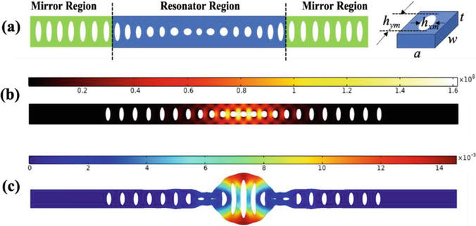
Figure 15.
(a) The schematic diagram of the plane-viewed silicon optomechanical crystal nanobeam cavity and unit cell geometry in the mirror region; (b)
Exploration of fundamental quantum physics and advancements in quantum information technologies greatly benefit from the significant role played by quantum entanglement in optomechanical systems. In this particular domain, we have reviewed the advancements in theory and experimentation concerning entangled states at a macroscopic level within optomechanical systems, and have provided insights into the future potential applications of this field [88]. The review also includes a concise introduction to key theoretical tools that aid in comprehending and addressing entanglement issues in opto-mechanics. Furthermore, we have introduced the entangling interaction between the electromagnetic fields and a mechanical oscillator, as well as that among multiple mechanical oscillators and that of electromagnetic fields associated with a mechanical oscillator. Additionally, we have summarized various approaches to mitigate the effect from thermal noise, which can enhance experimental feasibility and practical applicability. In conclusion, cryogenic environments will continue to play a pivotal role in future experimental studies in this field for an extended period. Maintaining quantum characteristics in more conventional settings will be an essential focus for practical applications in quantum optomechanical system.
5.3 Nano-opto-electro-mechanical system
The nano-opto-electro-mechanical system (NOEMS) is an emerging category of hybrid systems that integrate optical, electrical, and mechanical functionalities within nanoscale devices. Among them, graphene has emerged as a promising material for implementing mechanical resonators due to its exceptional characteristics, including lightweight composition, high-quality factors, and adjustable resonant frequencies. In our study, we have introduced a phonon laser operating at room temperature by utilizing an opto-mechanic cavity [89]. This cavity consisted of graphene and a silicon substrate forming an optical enclosure, with the added functionality of the graphene sheet serving as both the coupling mirror and the mechanical resonator.
The phonon dissipations decreased as the power of the pumping laser increased, and ceased when the pump power reached a sufficient level. Subsequently, the phonon transitioned into a state referred to as stimulated emission, resembling the process of photon lasing. The occurrence of phonon lasing was confirmed through observation of a distinct threshold in oscillation amplitude and a reduction in vibration mode linewidth. We anticipate that our discoveries will provide novel perspectives for developing functional devices based on mechanical graphene resonators and potentially find applications in quantum information processing.
Considering the 2D antiferromagnetic semiconductor chromium thiophosphate (CrPS4) for its excellent structure, photoelectric properties, and potential magnetic characteristics, we have experimentally studied the mechanical properties of layered CrPS4 and explored the resonance characteristics of a new few-layer CrPS4 nanomechanical resonator [90]. Figure 16 shows the material properties of layered CrPS4 and preparation of mechanical resonators in this work. The results exhibited exceptional vibration properties using the laser interferometry setup, showcasing the distinct resonant mode, capability to operate at extremely high frequency and gate tuning. Additionally, by analyzing temperature-regulated resonant frequencies, we successfully detected the magnetic phase transition of CrPS4 strips. This discovery validates the correlation between mechanical vibration and magnetic phase. These results lay a solid foundation for future exploration and utilization of 2D magnetic material resonators in quantum metrology research.
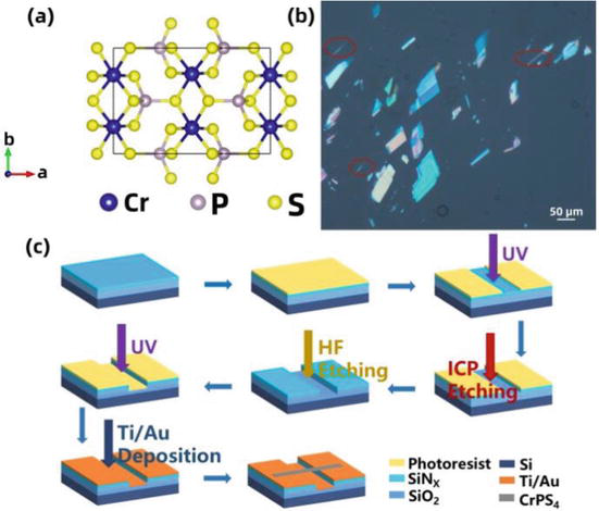
Figure 16.
Material properties of layered CrPS4 and preparation of mechanical resonators. (a) the crystal structure of CrPS4 is presented as an ab plane. (b) Layered CrPS4 obtained by mechanical exfoliation under optical microscope. (c) Detailed process flowchart of CrPS4 mechanical resonators. From ref. [
Given the extensive activity in this emerging field, we have reviewed recent advancements and significant accomplishments in NOEMSs, with a particular focus on the fundamental aspects of the hybrid system and its diverse range of applications [91]. Additionally, our review delves into the distinctions between classical information transduction and quantum information processing when applying NOEMS, thereby presenting an expanded scope for engineering and enhancing NOEMS within the realm of quantum mechanics.
6. Conclusion
In order to realize practical quantum systems in the future, our group have made efforts to create and investigate quantum devices by using optoelectronic techniques. QD-embedded nanocavities were designed to improve the efficiency of and to realize on demand single photon emitters. Spectral multiplexing technique enabled the fabrication of a heralded single photon source with high purity and speed, approaching on-demand single photon emitting. A quantum random number generator working at room temperature was constructed based on single-photon emission from defects in commercial GaN material. Applying cascaded second-order nonlinear optical process in PPLN waveguides, we developed an entangled photon emitter with visibility of 97% and noise level nearly 10 times better. Another photon entangler with visibility of over 99% was established using Si3N4 micro-rings. Readout circuits were optimized to help fabricating high-quality SPAD devices, and SPAD focal plane devices were improved to 128 × 32 array for single photon and quantum imaging. A quantum memory was achieved to simultaneously store 1650 single photons at low temperatures, and a few opto-electro-mechanical devices were experimentally tried to obtain quantum-level measurement ability for minor quantities. Our studies might be a step forward to the realization of practical quantum information networks.
Acknowledgments
This work was partially supported by the National Key Research and Development Program of China (Nos. 2018YFA0307400, 2018YFA0306102, 2019YFB2203400, 2021YFA0718803); Sichuan Science and Technology Program (Nos. 2020YFG0466, 2021YFSY0063, 2021YFSY0062, 2021YFSY0064, 2021YFSY0065, 2021YFSY0066, 2022YFSY0061, 2022YFSY0062, 2022YFSY0063); National Natural Science Foundation of China (Nos. U19A2076, 62005039); Innovation Program for Quantum Science and Technology (No. 2021ZD0301702); Chengdu Science and Technology Program No. 2021YF0800159GX; and the Rongpiao Plan of Chengdu city, China.
References
- 1.
Wu J, Huang Y, Lu C, Ding T, Zheng Y, Chen X. Tunable linear polarization-state generator of single photons on a lithium Niobate Chip. Physical Review Applied. 2020; 13 (6):064068. DOI: 10.1103/PhysRevApplied.13.064068 - 2.
Boschi D, Branca S, De Martini F, Hardy L, Popescu S. Experimental realization of teleporting an unknown pure quantum state via dual classical and Einstein-Podolsky-Rosen channels. Physical Review Letters. 1998; 80 (6):1121-1125. DOI: 10.1103/PhysRevLett.80.1121 - 3.
Bouwmeester D, Pan J-W, Mattle K, Eibl M, Weinfurter H, Zeilinger A. Experimental quantum teleportation. Nature. 1997; 390 (6660):575-579. DOI: 10.1038/37539 - 4.
O'Brien JL. Optical quantum computing. Science. 2007; 318 (5856):1567-1570. DOI: 10.1126/science.1142892 - 5.
Pan J-W, Gasparoni S, Ursin R, Weihs G, Zeilinger A. Experimental entanglement purification of arbitrary unknown states. Nature. 2003; 423 (6938):417-422. DOI: 10.1038/nature01623 - 6.
Pan J-W, Simon C, Brukner Č, Zeilinger A. Entanglement purification for quantum communication. Nature. 2001; 410 (6832):1067-1070. DOI: 10.1038/35074041 - 7.
Yamamoto T, Koashi M, Özdemir ŞK, Imoto N. Experimental extraction of an entangled photon pair from two identically decohered pairs. Nature. 2003; 421 (6921):343-346. DOI: 10.1038/nature01358 - 8.
Yao XC, Wang TX, Chen HZ, Gao WB, Fowler AG, Raussendorf R, et al. Experimental demonstration of topological error correction. Nature. 2012; 482 (7386):489-494. DOI: 10.1038/nature10770 - 9.
Gisin N, Ribordy G, Tittel W, Zbinden H. Quantum cryptography. Reviews of Modern Physics. 2002; 74 (1):145-195. DOI: 10.1103/RevModPhys.74.145 - 10.
Kasture S, Lenzini F, Haylock B, Boes A, Mitchell A, Streed EW, et al. Frequency conversion between UV and telecom wavelengths in a lithium niobate waveguide for quantum communication with Yb+ trapped ions. Journal of Optics. 2016; 18 (10):104007. DOI: 10.1088/2040-8978/18/10/104007 - 11.
Kimble HJ. The quantum internet. Nature. 2008; 453 (7198):1023-1030. DOI: 10.1038/nature07127 - 12.
Wehner S, Elkouss D, Hanson R. Quantum internet: A vision for the road ahead. Science. 2018; 362 (6412):eaam9288. DOI: 10.1126/science.aam9288 - 13.
Wei S-H, Jing B, Zhang X-Y, Liao J-Y, Yuan C-Z, Fan B-Y, et al. Towards real-world quantum networks: A review. Laser & Photonics Reviews. 2022; 16 (3):2100219. DOI: 10.1002/lpor.202100219 - 14.
Wengerowsky S, Joshi SK, Steinlechner F, Hübel H, Ursin R. An entanglement-based wavelength-multiplexed quantum communication network. Nature. 2018; 564 (7735):225-228. DOI: 10.1038/s41586-018-0766-y - 15.
Boyer V, Marino AM, Pooser RC, Lett PD. Entangled images from four-wave mixing. Science. 2008; 321 (5888):544-547. DOI: 10.1126/science.1158275 - 16.
Brida G, Genovese M, Ruo BI. Experimental realization of sub-shot-noise quantum imaging. Nature Photonics. 2010; 4 (4):227-230. DOI: 10.1038/nphoton.2010.29 - 17.
Giovannetti V, Lloyd S, Maccone L. Advances in quantum metrology. Nature Photonics. 2011; 5 (4):222-229. DOI: 10.1038/nphoton.2011.35 - 18.
Treps N, Grosse N, Bowen WP, Fabre C, Bachor H-A, Lam PK. A quantum laser pointer. Science. 2003; 301 (5635):940-943. DOI: 10.1126/science.1086489 - 19.
Bharadwaj D, Thyagarajan K. Direct generation of hybrid entangled photon pairs in waveguides. Journal of the Optical Society of America B. 2018; 35 (4):790-796. DOI: 10.1364/JOSAB.35.000790 - 20.
Kumar R, Ghosh J. Parametric down-conversion in ppLN ridge waveguide: A quantum analysis for efficient twin photons generation at 1550 nm. Journal of Optics. 2018; 20 (7):075202. DOI: 10.1088/2040-8986/aac7da - 21.
Kumar R, Ghosh J. SPDC photon pairs using a spatially anti-symmetric pump beam in a ppLN ridge waveguide. Applied Physics B. 2020; 126 (11):186. DOI: 10.1007/s00340-020-07537-x - 22.
Santandrea M, Stefszky M, Ansari V, Silberhorn C. Fabrication limits of waveguides in nonlinear crystals and their impact on quantum optics applications. New Journal of Physics. 2019; 21 (3):033038. DOI: 10.1088/1367-2630/aaff13 - 23.
Zhang K, He J, Wang J. Two-way single-photon-level frequency conversion between 852 nm and 1560 nm for connecting cesium D2 line with the telecom C-band. Optics Express. 2020; 28 (19):27785-27796. DOI: 10.1364/OE.402355 - 24.
IBM. The IBM quantum heavy hex lattice. 2021. Available from: https://research.ibm.com/blog/heavy-hex-lattice - 25.
Gambetta JM, Chow JM, Steffen M. Building logical qubits in a superconducting quantum computing system. npj Quantum Information. 2017; 3 :2. DOI: 10.1038/s41534-016-0004-0 - 26.
Beterov I. Quantum computers based on cold atoms. Optoelectronics, Instrumentation and Data Processing. 2020; 56 :317-324. DOI: 10.3103/S8756699020040020 - 27.
Zhang X, Li H-O, Cao G, Xiao M, Guo G-C, Guo G-P. Semiconductor quantum computation. National Science Review. 2019; 6 (1):32-54. DOI: 10.1093/nsr/nwy153 - 28.
Azuma H. Quantum computation with Kerr-nonlinear photonic crystals. Journal of Physics D: Applied Physics. 2008; 41 (2):025102. DOI: 10.1088/0022-3727/41/2/025102 - 29.
Wolters J, Buser G, Horsley A, Béguin L, Jöckel A, Jahn JP, et al. Simple atomic quantum memory suitable for semiconductor quantum dot single photons. Physical Review Letters. 2017; 119 :060502. DOI: 10.1103/PhysRevLett.119.060502 - 30.
Lamata L. Quantum and optoelectronic devices, circuits and systems. Electronics. 2023; 12 (7):1717. DOI: 10.3390/electronics12071717 - 31.
Michaelis de Vasconcellos S, Gordon S, Bichler M, et al. Coherent control of a single exciton qubit by optoelectronic manipulation. Nature Photon. 2010; 4 :545-548. DOI: 10.1038/nphoton.2010.124 - 32.
Kimura S, Kumano H, Endo M, Suemune I, Yokoi T, Sasakura H, et al. Photon Antibunching observed from an InAlAs single quantum dot. Japanese Journal of Applied Physics. 2005; 44 (6L):L793. DOI: 10.1143/JJAP.44.L793 - 33.
Cheng R, Huang S, Xu Q , Xie X, Zhang W, Zhou Q , et al. Research progress of lithium niobate waveguide and its application in quantum information technology. In: 2021 Photonics & Electromagnetics Research Symposium (PIERS); 21-25 November 2021. Hangzhou, China: IEEE; 2021. pp. 877-896 - 34.
Wrachtrup J, Jelezko F. Processing quantum information in diamond. Journal of Physics: Condensed Matter. 2006; 18 (21):S807. DOI: 10.1088/0953-8984/18/21/S08 - 35.
Kagan CR, Bassett LC, Murray CB, Thompson SM. Colloidal quantum dots as platforms for quantum information science. Chemical Reviews. 2021; 121 (5):3186-3233. DOI: 10.1021/acs.chemrev.0c00831 - 36.
Liu X, Hersam MC. 2D materials for quantum information science. Nature Reviews Materials. 2019; 4 :669-684. DOI: 10.1038/s41578-019-0136-x - 37.
Cao Z-L, Hu F-R, Zhang C-F, Zhu S-N, Xiao M, Wang X-Y. Optical studies of semiconductor perovskite nanocrystals for classical optoelectronic applications and quantum information technologies: A review. Advanced Photonics. 2020; 2 (5):054001. DOI: 10.1117/1.AP.2.5.054001 - 38.
Grimsmo AL, Royer B, Kreikebaum JM, Ye Y, O’Brien K, Siddiqi I, et al. Quantum metamaterial for broadband detection of single microwave photons. Physical Review Applied. 2021; 15 :034074. DOI: 10.1103/PhysRevApplied.15.034074 - 39.
Kumano H, Kimura S, Endo M, Suemune I, Sasakura H, Adachi S, et al. Triggered single-photon emission and cross-correlation properties in InAlAs quantum dot. Physica E: Low-dimensional Systems and Nanostructures. 2006; 32 (1):144-147. DOI: 10.1016/j.physe.2005.12.027 - 40.
Takemoto K, Nambu Y, Miyazawa T, Wakui K, Hirose S, Usuki T, et al. Transmission experiment of quantum keys over 50 km using high-performance quantum-dot single-photon source at 1.5 μm wavelength. Applied Physics Express. 2010; 3 (9):092802. DOI: 10.1143/APEX.3.092802 - 41.
Song H-Z, Hadi M, Zheng Y, Shen B, Zhang L, Ren Z, et al. InGaAsP/InP Nanocavity for single-photon source at 1.55-μm telecommunication band. Nanoscale Research Letters. 2017; 12 (1):128. DOI: 10.1186/s11671-017-1898-y - 42.
Huang S, Xie X, Xu Q , Zhao X, Deng G, Zhou Q , et al. Fabrication tolerance of InGaAsP/InP-air-aperture micropillar cavities as 1.55-μm quantum dot single-photon sources. Current Optics and Photonics. 2020; 4 (6):509-515. DOI: 10.3807/COPP.2020.4.6.509 - 43.
Yu H, Yuan C, Zhang R, Zhang Z, Li H, Wang Y, et al. Spectrally multiplexed indistinguishable single-photon generation at telecom-band. Photonics Research. 2022; 10 (6):1417-1429. DOI: 10.1364/PRJ.450731 - 44.
Fan Y-R, Yuan C-Z, Zhang R-M, Shen S, Wu P, Wang H-Q , et al. Effect of dispersion on indistinguishability between single-photon wave-packets. Photonics Research. 2021; 9 (6):1134-1143. DOI: 10.1364/PRJ.421180 - 45.
Luo Q , Cheng Z, Fan J, Tan L, Song H, Deng G, et al. Quantum random number generator based on single-photon emitter in gallium nitride. Optics Letters. 2020; 45 (15):4224-4227. DOI: 10.1364/OL.396561 - 46.
Meyer-Scott E, Silberhorn C, Migdall A. Single-photon sources: Approaching the ideal through multiplexing. Review of Scientific Instruments. 2020; 91 :041101. DOI: 10.1063/5.0003320 - 47.
Song H-Z. The development of quantum emitters based on quantum dots-a chapter. In: Yu P, Wang ZM, editors. Quantum Dot Optoelectronic Devices. Switzerland AG: Springer Nature; 2020. Chapter 3. pp. 83-106. DOI: 10.1007/978-3-030-35813-6 - 48.
Song H-Z, Takemoto K, Miyazawa T, Takatsu M, Iwamoto S, Yamamoto T, et al. Design of Si/SiO2 micropillar cavities for Purcell-enhanced single photon emission at 1.55 μm from InAs/InP quantum dots. Optics Letters. 2013; 38 :3241. DOI: 10.1364/OL.38.003241 - 49.
Song H-Z, Takemoto K, Miyazawa T, Takatsu M, Iwamoto S, Ekawa M, et al. High quality-factor Si/SiO2-InP hybrid micropillar cavities with submicrometer diameter for 1.55-μm telecommunication band. Optics Express. 2015; 23 (12):16264-16272. DOI: 10.1364/OE.23.016264 - 50.
Xie X-M, Xu Q , Shen B-Z, Chen J, Dai Q , Shi Z, et al. InGaAsP/InP micropillar cavities for 1.55 μm quantum-dot single photon sources. In: 6th Conference on Advances in Optoelectronics and Micro/Nano-Optics; 23-26 April 2017. Vol. 844(1). Nanjing, China: IOP Publishing; 2017. p. 012002 - 51.
Guo S-J, Zheng Y-Z, Weng Z, Yao H-C, Ju Y-H, Zhang L, et al. InGaAsP/InP-air-aperture microcavities for single-photon sources at 1.55-μm telecommunication band. In: Nanophotonics and Micro/Nano Optics III; 4 November 2016. Beijing, China: SPIE; 2016. DOI: 10.1117/12.2247841 - 52.
Song H-Z, Zhang W, Yu L-B, Wang Z-M. Micropillar cavity design for 1.55-μm quantum-dot single-photon sources. Journal of Electronic Science and Technology. 2019; 17 (3):221. DOI: 10.11989/JEST.1674-862X.71027010 - 53.
Song H-Z. Microcavities for silica-fiber based quantum information processing. In: Pyshkin S, Ballato J, editors. Optoelectronics – Advanced Device Structures. London, UK, Crotia: Intech, Chapter 2; 2017. pp. 21-48. DOI: 10.5772/67499 - 54.
Cheng R, Huang S, Xu Q , Xie X-M, Zhang W, Zhou Q , et al. Research Progress of lithium Niobate waveguide and its application in quantum information technology. In: IEEE Xplore/2021 Photonics & Electromagnetics Research Symposium (PIERS); 21-25 November 2021. Hangzhou, China: IEEE; 2022. pp. 877-896 - 55.
Huang S, Zhang W, Xi Q , Zhao XH, Xie X, Xu Q , et al. Robustness of Si/SiO2-InP micropillar cavity for 1.55-μm single photon source. Laser Technology. 2020; 44 (5):532-537 (in Chinese) - 56.
Jennewein T, Simon C, Weihs G, Weinfurter H, Zeilinger A. Quantum cryptography with entangled photons. Physical Review Letters. 2000; 84 (20):4729-4732. DOI: 10.1103/PhysRevLett.84.4729 - 57.
Mitchell MW, Lundeen JS, Steinberg AM. Super-resolving phase measurements with a multiphoton entangled state. Nature. 2004; 429 (6988):161-164. DOI: 10.1038/nature02493 - 58.
Sun Q-C, Mao Y-L, Chen S-J, Zhang W, Jiang Y-F, Zhang Y-B, et al. Quantum teleportation with independent sources and prior entanglement distribution over a network. Nature Photonics. 2016; 10 (10):671-675. DOI: 10.1038/nphoton.2016.179 - 59.
Jin R-B, Cai N, Huang Y, Hao X-Y, Wang S, Li F, et al. Theoretical investigation of a spectrally pure-state generation from isomorphs of KDP crystal at near-infrared and telecom wavelengths. Physical Review Applied. 2019; 11 (3):034067. DOI: 10.1103/PhysRevApplied.11.034067 - 60.
Li J, Yuan C, Shen S, Zhang Z, Zhang R, Li H, et al. Discrete frequency-bin entanglement generation via cascaded second-order nonlinear processes in Sagnac interferometer. Optics Letters. 2023; 48 (11):2917-2920. DOI: 10.1364/OL.489656 - 61.
Zhang Z, Yuan C, Shen S, Yu H, Zhang R, Wang H, et al. High-performance quantum entanglement generation via cascaded second-order nonlinear processes. npj Quantum Information. 2021; 7 (1):123. DOI: 10.1038/s41534-021-00462-7 - 62.
Fan Y-R, Lyu C, Yuan C-Z, Fan B-Y, Jing B, Zhou D-L, et al. Multi-wavelength correlated photon pairs generation in Si3N4 microring resonator. In: 2021 IEEE 6th Optoelectronics Global Conference (OGC); 15-18 September 2021. Shenzhen. China: IEEE; 2021. pp. 100-102 - 63.
Fan Y-R, Lyu C, Yuan C-Z, Deng G-W, Zhou Z-Y, Geng Y, et al. High-quality multi-wavelength quantum light sources on silicon nitride micro-ring chip. arXiv[quant-ph]. 2022; 2209 :11417. DOI: 10.48550/arXiv.2209.11417 - 64.
Shen S, Yuan C-Z, Zhang Z-C, Wang H-Q , Li H, You L-X, et al. High-performance quantum teleportation Systems at Telecom C-band. In: Conference on Lasers and Electro-Optics; 09 May 2021. San Jose, California: Optica Publishing Group; 2021. p. FM3M.2 - 65.
Shen S, Yuan C, Zhang Z, Yu H, Zhang R, Yang C, et al. Hertz-rate metropolitan quantum teleportation. Light: Science & Applications. 2023; 12 (1):115. DOI: 10.1038/s41377-023-01158-7 - 66.
Fan Y-R, Luo Y, Zhang Z-C, Li Y-B, Liu S, Wang D, et al. Energy-time Entanglement Coexisting with Fiber Optical Communication at Telecom C-band. arXiv[quant-ph]. 2023; 2305 :18696. DOI: 10.48550/arXiv.2305.18696 - 67.
Cheng B-T, Dai Q , Xie X-M, Xu Q , Zhang S, Song H-Z. Research progress of single-photon detectors. Laser Technology. 2022; 46 (5):601. DOI: 10.7510/jgjs.issn.1001-3806 (in Chinese) - 68.
Yuan F, Lu XL, Jing L, Yang YX, Kong FL, Deng SJ, et al. A novel high-speed photon counting system with programmed dead time. In: 2019 IEEE 4th Optoelectronics Global Conference (OGC); 3-6 September 2019. Shenzhen, China: IEEE; 2019. pp. 85-88 - 69.
Song H-Z, Deng J, Dai Q , Shi Z, Yu L-B. Quantitative correlation between fabrication precision and device homogeneity of single-photon avalanche diodes. IEEE Transactions on Electron Devices. 2016; 63 (12):4845-4851. DOI: 10.1109/TED.2016.2618222 - 70.
Zhang S, Yuan F, Chen J, Xie X, Xu Q , Cheng B, et al. Research progress of negative feedback avalanche diode and its application. In: 2nd International Conference on Laser, Optics and Optoelectronic Technology (LOPET 2022); 20-22 May 2022. Qingdao, China: SPIE; 2022. pp. 182-191 - 71.
Huang X, Cao Q , Wan M, Song H-Z. Electronic and optical properties of BP, InSe monolayer and BP/InSe heterojunction with promising photoelectronic performance. Materials. 2022; 15 (18):6214. DOI: 10.3390/ma15186214 - 72.
Fan X, Ou Z, Zhang L, Zhang R, Yuan C, Deng G, et al. Dense temporally multiplexed Fiber Bragg grating sensing based on single-photon detection. Journal of Lightwave Technology. 2022; 40 (13):4458-4466. DOI: 10.1109/JLT.2022.3158074 - 73.
Ou Z, Fan X, Zhang L, Fan Y, Yuan C, You L, et al. Effect of spectrum broadening on photon-counting fiber Bragg grating sensing. Optics Express. 2023; 31 (5):8152-8159. DOI: 10.1364/OE.482821 - 74.
Song H-Z. Avalanche photodiode focal plane arrays and their application in laser detection and ranging. Chapter 9, in Advances Photodiodes - Research and Applications, ed. Kuan Chee, ISBN 978-953-51-6779-2, London, UKIntechOpen. 2018. - 75.
Zheng-Ping LI, Huang X, Jiang P-Y, Hong Y, Yu H, Cao Y, et al. Super-resolution single-photon imaging at 8.2 kilometers. Optics Express. 2020; 28 (3):4076. DOI: 10.1364/OE.383456 - 76.
Itzler MA, Jiang X, Nyman B, et al. InP-based negative feedback avalanche diodes. In: Quantum Sensing and Nanophotonic Devices VI; 26 January 2009. Vol. 7222. California, United States: SPIE; 2009. pp. 462-473 - 77.
Yuan F, Lu X, Ke Z, Xie X, Liu Q, Yang Y, et al. A design of near-infrared single photon counting integrated module based on InGaAs/InP NFAD. Proceedings of SPIE. 2023; 12781 :127810Y. DOI: 10.1117/12.2687239 - 78.
Cheng B-T, Zho Y, Jiang R-M, Wang X-L, Huang S, Huang X-Y, et al. Structural, electronic and optical properties of some new Trilayer Van de Waals Heterostructures. Nanomaterials. 2023; 13 :1574. DOI: 10.3390/nano13091574 - 79.
Miao J, Wang C. Avalanche photodetectors based on two-dimensional layered materials. Nano Research. 2021; 14 :1878-1888. DOI: 10.1007/s12274-020-3001-8 - 80.
Zhang J, Itzler MA, Zbinden H, Pan J-W. Advances in InGaAs/InP single-photon detector systems for quantum communication. Light: Science & Applications. 2015; 4 (5):e286-e. DOI: 10.1038/lsa.2015.59 - 81.
Grobnic D, Smelser CW, Mihailov SJ, Walker RB. Long-term thermal stability tests at 1000 °C of silica fibre Bragg gratings made with ultrafast laser radiation. Measurement Science and Technology. 2006; 17 (5):1009. DOI: 10.1088/0957-0233/17/5/S12 - 82.
Wei Z, Song D, Zhao Q , Cui HL. High pressure sensor based on Fiber Bragg grating and carbon Fiber laminated composite. IEEE Sensors Journal. 2008; 8 (10):1615-1619. DOI: 10.1109/JSEN.2008.929070 - 83.
Gusarov AI, Berghmans F, Deparis O, Fernandez AF, Defosse Y, Megret P, et al. High total dose radiation effects on temperature sensing fiber Bragg gratings. IEEE Photonics Technology Letters. 1999; 11 (9):1159-1161. DOI: 10.1109/68.784237 - 84.
Xi Q , Wei S, Yuan C, Zhang X, Wang Y, Song H, et al. Experimental observation of coherent interaction between laser and erbium ions ensemble doped in fiber at sub 10 mK. Science China Information Sciences. 2020; 63 (8):180505. DOI: 10.1007/s11432-020-2954-5 - 85.
Wei S-H, Jing B, Zhang X-Y, Liao J-Y, Li H, You L-X, et al. Storage of 1650 modes of single photons at telecom wavelength. 2022. DOI: 10.48550/arXiv.2209.00802 - 86.
Lv X, Fan B, Tang J, Xu N, Chen H, Zhang Y, et al. The influence of fabrication imperfections in an optomechanical crystal nanobeam cavity. In: Asia Communications and Photonics Conference/International Conference on Information Photonics and Optical Communications 2020 (ACP/IPOC); 24 October 2020. Beijing, China: Optica Publishing Group; 2020. p. M4A.19 - 87.
Cai Q , Fan B, Fan Y, Deng G, Wang Y, Song H, et al. Entangling optical and mechanical cavity modes in optomechanical crystal nanobeam. Physical Review A. 2023; 108 (2):022419. DOI: 10.1103/PhysRevA.108.022419 - 88.
Tang J-D, Cai Q-Z, Cheng Z-D, Xu N, Peng G-Y, Chen P-Q , et al. A perspective on quantum entanglement in optomechanical systems. Physics Letters A. 2022; 429 :127966. DOI: 10.1016/j.physleta.2022.127966 - 89.
Li W-J, Cheng Z-D, Kang L-Z, Zhang R-M, Fan B-Y, Zhou Q , et al. Phonon lasing with an atomic thin membrane resonator at room temperature. Optics Express. 2021; 29 (11):16241-16248. DOI: 10.1364/OE.423904 - 90.
Li B-L, Guo M-L, Chen J-F, Fang J-W, Fan B-Y, Zhou Q , et al. Very high-frequency, gate-tunable CrPS4 nanomechanical resonator with single mode. Optics Letters. 2023; 48 (10):2571-2574. DOI: 10.1364/OL.489345 - 91.
Xu N, Cheng Z-D, Tang J-D, Lv X-M, Li T, Guo M-L, et al. Recent advances in nano-opto-electro-mechanical systems. Nano. 2021; 10 (9):2265-2281. DOI: 10.1515/nanoph-2021-0082