Open access peer-reviewed chapter

Optical Response of 3D Model Topological Nodal-Line Semimetal

Written By

Sita Kandel, Godfrey Gumbs and Oleg L. Berman

Submitted: 24 January 2023 Reviewed: 13 March 2023 Published: 28 June 2023

DOI: 10.5772/intechopen.1001440

From the Edited Volume

Advances in Nanosheets - Preparation, Properties and Applications

Dr. Karthikeyan Krishnamoorthy

Chapter metrics overview

68 Chapter Downloads

View Full Metrics

Abstract

We present a semi-analytical expression for both longitudinal and transverse optical conductivities of a model TNLSM employing the Kubo formula with emphasis on the optical spectral weight redistribution, deduced from appropriate Green’s functions. In this semimetal, the conduction and valence bands cross each other along a one- dimensional curve protected by certain symmetry group in the 3D Brillouin zone. Although the crossing cannot be removed by any perturbations, it can be adjusted by continuous tuning of the Hamiltonian with a parameter α. When α>0, the two bands cross each other near the Γ point in the (kx,ky) plane of the first Brillouin zone making a nodal circle of radius α. The circle shrinks to point when α=0 and for α<0, the nodal circle vanishes and a gap opens around Γ. Numerical results for the longitudinal optical response of such TNLSM are investigated by varying the gap due to modifying α, the chemical potential μ, temperature T and the dephasing parameter η. The longitudinal optical conductivity is anisotropic along the direction parallel or perpendicular to the nodal ring. However, the transverse optical conductivity vanishes due to rotational symmetry.

Keywords

  • optical conductivity
  • nodal-line semimetal
  • topologically protected material
  • anisotropic energy band
  • linear response theory

1. Introduction

In recent times, topological semimetals (TSM) have come to the forefront of condensed matter physics following precise theoretical predictions, well controlled material synthesis and advance characterized techniques such as angle-resolved photoemission spectroscopy (ARPES), scanning tunneling microscopy (STM), and optical spectroscopy [1, 2, 3, 4]. The ARPES directly probes the band structures of bulk and surface states, and information on the Fermi surface can also be revealed by STM through the quasiparticle interference process. Variety of TSM has been theoretically predicted and experimentally confirmed including Weyl [5], Dirac [6], and nodal-line semimetals [7], which correspond to different types of band crossings and the associated band topologies [8]. For these systems, the conduction and valence bands cross each other in the Brillouin zone (BZ). It is important to note that the crossing cannot be eliminated by perturbing the Hamiltonian without breaking either its crystalline or time-reversal symmetry. Therefore, all topological semimetals belong to symmetry protected topological phases of matter.

For Dirac semimetals, the conduction and valence bands have linear crossing at the Dirac point. If the time-reversal symmetry is broken, the Dirac point splits into two separated ones, and the system becomes a Weyl semimetal. On the other hand, for the nodal-line semimetal, the crossing of the valence and conduction bands forms a nodal ring (also called nodal line). The NLSM exhibit some peculiar properties which are absent in Dirac and Weyl semimetals. For example, the single nodal line in the NLSM can shrink to a point and vanish by continuously tuning the Hamiltonian in the absence of spin-orbital coupling (SOC). When strong SOC is added to the system, each nodal-line is either split or gapped due to hybridization between opposite spin components [9]. It is not true for the four bands crossing nodal-line for which the nodal-line is preserved even in the strong SOC regime and cannot be completely gapped out by tuning the Hamiltonian. In this work, we consider the two-bands crossing NLSM in the absence of SOC.

The surface states of topological materials are significantly affected by the number of layers and impurities. When the number of material layers is insufficient, the surface state will not be formed, or impurities in the system can readily destroy the surface states. In general, observation of surface states of topological materials such as drum-head surface states (DSS) of NLSM [2, 10, 11, 12, 13, 14] is still a great challenge. Our current work mainly focuses on the physical properties of bulk states.

When it came to be known that some topological semimetals exhibit different energy band dispersion relations than those of Dirac and Weyl materials, and making a nodal ring at the cross-section of the valence and conduction bands, NLSM have offered an attractive research platform for exploring a variety of novel phenomena. Various materials have been theoretically predicted or experimentally confirmed as NLSM, including ZrXY (X = Si, Ge, Y = S, Se, Te) [3, 15, 16], graphene networks [14], compressed black phosphorus [17] as well as HgCr2Se4 [18]. The optical conductivity of monolayer and bilayer graphene, and few-layer epitaxial graphite has been reported recently [19]. These studies have yielded useful information regarding the electron dynamics. We refer to reference [20] for a review of other remarkable properties of these TSM systems as well as a discussion of possible technological applications. Here, we consider the optical conductivity of a NLSM model system with special emphasis on the optical spectral weight redistribution due to changes in the chemical potential caused by charging as well as an adjustable parameter α which governs the degree of crossing between the valence and conduction bands. The parameter α can be manipulated by strain. The effect of mechanical strain on the optical properties of nodal-line semimetal ZrSiS has been studied using first-principles calculations in Ref. [21]. According to reference [21], frequency-independent optical conductivity is robust with respect to uniaxial compressive strain of up to 10 GPa.

Similar studies have reported previously. In 2016/17, Carbotte and his team [22, 23] studied the optical response of 3D NLSM and came to the conclusion that it presents two-dimensional (2D) Dirac-like response in the low-photon energy regime and 3D Dirac-like response in the high-energy photon limit. Later on in 2017, Sashin Barati [24] also showed that the optical conductivity of NLSM is anisotropic. Both those authors considered different toy models in order to explain NLSM with different Fermi surfaces. However, none of these results totally agree with the paper by Habe and Koshino [25]. Koshino and his team studied theoretically the dynamical conductivity of ZrSiS by using a multi-orbital tight-binding model based on a first-principles band calculation. According to Habe and Koshino, ZrSiS type NLSM attributes the optical conductivity which is neither liner like 2D- nor like 3D. The interband contribution first increases slowly for some frequency range, then it is decreased to smaller value and saturates for large frequency. This motivates us to study the optical response of similar materials using a simple model Hamiltonian and the Kubo formula which yields semi-analytic results. We successfully presented semi-analytical formula for both transverse and longitudinal optical conductivity including both intra and interband contributions of the model Hamiltonians. Our result is interesting because the numerical solutions closely resemble Habe and Koshino’s results and are neither like 2D nor 3D Dirac or Weyl semimetal. The transverse optical conductivity of NLSM is found to vanish due to rotational symmetry along the ring of NLSM. This result is also supported by a recent study of Wang [26], who demonstrated the anomalous Hall optical conductivity in tilted topological nodal-line semimetals.

The rest of this work is organized as follows. In section II, we present the theoretical formalism for the calculation of the optical conductivity based on the simplest nearest-neighbor Hamiltonian. This model involves an adjustable parameter α associated with a nodal circle which may shrink to a point when α=0. Here, we have managed to derive a conveniently simple semi-analytical expression for the frequency-dependent conductivity for arbitrary chemical potential, making this a convenient result for experimentalists. In section III, we present numerical results demonstrating the anisotropy of the system, the α-dependence and charging pertaining to the biasing of the NLSM sample. Section IV is devoted to a summary of our results.

Advertisement

2. Theoretical background

The NLSM is modeled by a slab consisting of several nanosheets of single atoms along the
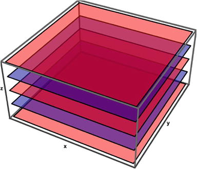
 z axis. We apply periodic boundary conditions along the z axis since we are only interested in bulk properties of the NLSM. This is shown schematically in Figure 1. Consequently, in this work, only bulk states are included in our calculations and not drum head surface states which arise for a slab of finite thickness. Such topologically protected DSS can be exhibited in a slab geometry with suitable thickness, e.g., with sixty unit cells for Ca3P2 [27].

Figure 1.

Schematic representation of a nodal-line semimetal consisting of several nanosheets of atoms stacked along the z axis making up a slab (color online).

Let us consider a Hamiltonian for which the nodal-line is stable against perturbations. However, the nodal-line may still shrink continuously to a point. In this regard. We turn to a single-spin effective Hamiltonian of a material such as ZrSiSe and ZrSiTe [3, 4]. In Ref. [2], the band structure of ZrSiTe was obtained using ab initio calculations. The idea here is to carry out a calculation based on a model Hamiltonian which mimics the essential features of the true band structure near the Γ point of a NLSM such as ZrSiTe. In general, these band structures obtained from first-principles calculations or the generalized tight-binding model are very complicated. Of course, not all features are reproduced by this model Hamiltonian throughout the Brillouin zone but it could serve as a useful tool for generating qualitative results to get a better understanding of this growing class of topological semimetals. For the nodal line, enclosed with either a ring or a sphere, the symmetry group Z2 is the topological classification of the wave functions on the ring/sphere [20]. Therefore, a nodal ring is characterized by two independent Z2 indices, denoted by ζ1 and ζ2, defined on a ring that links with the line and on a sphere that encloses the whole line. According to reference [20], all topological nodal rings, protected by this symmetry group with respect to an arbitrarily small perturbation, are characterized by ζ1=1. For NLSMs with ζ1=1 and ζ2=0, our toy model Hamiltonian is given by [20]

Ĥ=αk2σ̂z+kzσ̂x,E1

where energy is measured in units of vFkF with vF the Fermi velocity equal to 106m/s and kF is the Fermi wave vector. Also, the wave vector k=kxkykz is scaled in terms of π/a where a is a lattice constant and 1ki1 with i=x,y,z in order to ensure that the model is restricted near the Γ point. For convenience, we will refer to this hypercubic region as the Brillouin zone. We have σ̂x,σ̂z representing Pauli matrices. The quantity α is an adjustable parameter which can be employed to vary the energy gap around the Γ point for which the energy bands are given by

εsk=skz2+αk22.E2

The band degeneracy occurs as
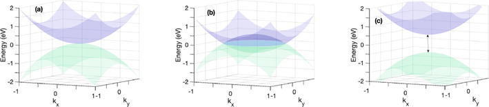
 kx2+ky2=α and kz=0. The two bands touch at k=0 when α=0. If α>0, the two subbands cross each other near the Γ point on the kxky plane for fixed kz=0, describing a nodal circle of radius α which shrinks to a point at k=0 as α is decreased to zero and the nodal circle vanishes and the valance and conduction bands are gapped out when α<0. The 3D energy dispersion is presented in Figure 2. In Figure 3, we plot the energy bands in the first BZ hypercube along lines joining points of high symmetry, corresponding to α=0 and α=0.5. These two contrasting cases demonstrate how the band gap near Γ may be tuned by varying this parameter which may be manipulated as a function of strain. It is clear from these results that the band structure is modified by finite α throughout the BZ. Figure 3(b) shows that the bulk band gap closes at an even number of discrete points near the Γ point. These special gap closing points in the BZ are protected by crystalline symmetry and play a role in the behavior of Weyl semimetals [28]. The detailed analysis of the topology of NLSMs, corresponding to the Hamiltonian in Eq. (1), is provided in [20]. This modification of the band structure has significant effects on the physical properties we calculate in this paper and may also affect the thermoelectric and Boltzmann transport as well as the plasmon excitations.

Figure 2.

(color online) the 3D contour energy bands of the NLSM described by the model Hamiltonian in
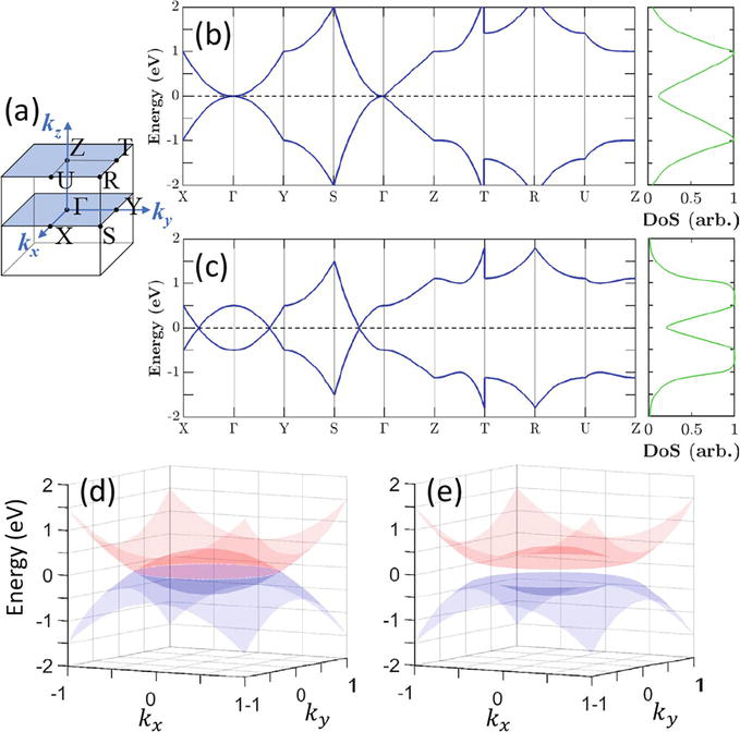
 Eq. (1) on the kz=0 plane for (a) α=0, (b) α=0.5 and (c) α=0.5. For positive α, two bands cross each other making a nodal circle of radius α. For α equal to zero, the nodal circle shrink to a point and for α<0, the nodal circle vanishes and the bands are gapped out.

Figure 3.

(color online) (a) shows the 3D hypercube, or reduced Brillouin zone, with its high-symmetry points for bulk NLSM. Bulk band structures between the high symmetry points (left) and corresponding density of states (right) for (b) α=0 and (c) α=0.5. The 3D contour bands are shown at low energy on the selected (kx,ky) plane for (d) kz=0 and (e) kz=0.2.

The normalized eigenvectors φs (for s=±) of the Hamiltonian (1) are given by

φsk=βskηskeikrV,E3

where V is a normalization volume. and βs and ηs are given by

βs2k=kz2kz2+k2α+sk2α2+kz22;E4
ηs2k=k2α+sk2α2+kz22kz2+k2α+sk2α2+kz22,E5

where βs and ηs satisfy the normalization condition: βs2+ηs2=1.

For the density-of-states, we have

Nω=NfBZd3k2π3s=±δωεsk.E6

We now introduce the Green’s function defined by Ĝ1z=zÎĤ which in matrix form is written as

Ĝωk=1Dωkω+αk2kzkzωαk2,E7

with Dωkω2αk22kz2=ωε+kωεk.

Now, the spectral function representation of the Green’s function is for i,j=1,2

Gijz=dω2πAijωzω.E8

For i,j=1,

G11z=dωA11ω2πzω=z+αk2zε+zεE9

Resolving the right-hand side of this equation into partial fractions, we obtain

1ε+εε++αk2zε+ε+αk2zε=dωA11ω2πzω=G11ω.E10

From this, we deduce

A11kω=2πε+εε++αk2δωε+ε+αk2δωε.E11

Similarly, we can obtain other spectral functions as follows.

A22kω=2πε+εε+αk2δωε+εαk2δωε,A12kω=A21kω=2πkzε+εδωε+δωε.E12

The real (absorptive) part of the optical conductivity can be written in the form

σαβΩ=Nfe22Ω2πfωμfω+Ωμ×BZd3k2π3Trv̂αÂkω+Ωv̂βÂ(kω),E13

where Nf is a degeneracy factor for the spin and at temperature T, we have fx=1/expx/T+1 as the Fermi function and μ is the chemical potential. Also, α,β represent spatial coordinates x,y,z. In doing our numerical calculations, we choose the zero temperature case T = 0 K, and the finite temperature case T = 300 K. For the longitudinal in-plane conductivity, σ̂xxΩ, we have v̂α=v̂β=v̂x=2kxσ̂z. Putting these results together, we conclude that the longitudinal conductivity σxxΩ is

σxxΩ=Nfe28ℏΩπ4μΩμBZd3kkx2γkωΩ,E14

where

γkω;Ω4π2{1kz2Ek2δω+ΩEkδωEk+δω+Ω+Ekδω+Ek+kz2Ek2δω+ΩEkδω+Ek+δω+Ω+EkδωEk}.E15

For temperature T=0 K, the Fermi function acts as a step function so the integration limit changes to μΩ to μ. In order to simplify the expressions, we chose Ek to represent the magnitude of energy eigenvalue. Hence, we replaced ε+k=Ek and εk=Ek. These terms give the intraband and interband contributions to the conductivity due to transitions within the conduction band and from transitions between the valence and conduction bands, respectively. The significance of these contributions is determined by the level of doping, the frequency Ω and implicitly by α through the energy dispersion εsk. The limit when Ω0 corresponds to the Drude conductivity [29]. We analyzed this intraband (Drude) conductivity using a Lorentzian representation for the δ-function. Additionally, the terms proportional to 1kz2/E2 in Eq. (15) vanish when Ω>0 and gives only the intraband conductivity.

Similarly, for α = β = y, we have v̂α=v̂β=v̂y=2kyσ̂z. The expression for σyyΩ comes out to be

σyyΩ=Nfe22Ω2πfωμfω+ΩμBZd3k2π32ky2γkωΩ.E16

Additionally, for α = β = z, we have v̂α=v̂β=v̂z=2kzσ̂z+σ̂x. The σzzΩ is

σzzΩ=Nfe22Ω2πfωμfω+ΩμBZd3k2π32kz2γkω;Ω4kzκkω;Ω+ζkω;Ω,E17

where

κkω;Ω4π2kzαk2Ek2{δω+ΩEkδωEkδω+Ω+EkδωEkδω+ΩEkδω+Ek+δω+Ω+Ekδω+Ek},E18
ζkω;Ω4π2{1kz2Ek2δω+ΩEkδω+Ek+δω+Ω+EkδωEk+kz2Ek2δω+ΩEkδωEk+δω+Ω+Ekδω+Ek}.E19

All three functions γ,κ and ζ are even functions of k=kxkykz.

For the transverse component σxyΩ, we must set α=x, β=y, v̂α=v̂x=2kxσ̂z and v̂β=v̂y=2kyσ̂z Then we obtain

σxyΩ=Nfe22Ω2πfωμfω+Ωμd3k2π34kxkyγkωΩ.E20

Since the integrand of σxy is an odd function of kx, the transverse component of the conductivity along kxky is zero. Similarly, for σyzΩ, setting α=y, β=z, v̂α=v̂y=2kyσ̂z and v̂β=v̂z=2kzσ̂z+σ̂x and for σxzΩ, setting α=x, β=z, v̂α=v̂x=2kxσ̂z and v̂β=v̂z=2kzσ̂z+σ̂x we arrive at

σyzΩ=Nfe22ℏΩ2πfωμfω+ΩμBZd3k2π32kyκkω;Ω+4kykzγkω;Ω,E21
σxzΩ=Nfe22ℏΩ2πfωμfω+ΩμBZd3k2π3{2kxκkωΩ+4kxkzγkωΩ.E22

Clearly, the integrands in Eq. (21) and Eq. (22) are both odd functions of kx and ky thereby making σyzΩ and σxzΩ zero. We now employ these results in the following section to carry out our numerical calculations for the longitudinal optical conductivity. These results exhibit the anisotropy of this NLSM system and demonstrate their dependence on the parameter α and the chemical potential μ as the frequency is varied.

Advertisement

3. Results and discussion for the longitudinal conductivity

We now examine in detail with the help of our numerical solutions the absorptive part of the longitudinal optical conductivity of an anisotropic nodal-line semimetal along the radial
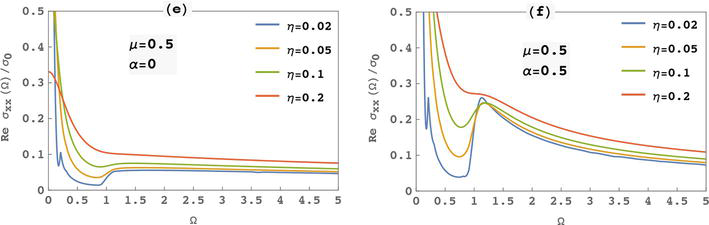
 x, y and axial z directions. For these calculations, we have used Nf=2 corresponds to spin degeneracy, the small momentum cutoff with 1kx,y,z1 to lie within a hypercube or so-called first Brillouin zone and a Lorentzian representation for the Dirac δ-function, i.e., δxηπ1η2+x2 with a broadening parameter η. This broadening takes into account the scattering due to non-magnetic impurities and lattice defects. The broadening is manifested in the optical conductivity as an effective transport scattering rate of 1τ=2η. In Figure 4, the effect of the broadening parameter η on the optical conductivity has been illustrated. All of the presented results are calculated for η=0.5. It is convenient to scale the conductivity by σ0=e2/4 and we set =1 in the above Kubo formula. The finite temperature responses are also analyzed using the Fermi-Dirac distribution function at temperature T by

Figure 4.

(color online) real part of the longitudinal optical conductivity at T = 0 K along x axis measured for μ=0.5 and for α=0 in (e) and for α=0.5 in (f). The different curves correspond to chosen dephasing parameter η. In the Lorentzian representation of the delta function, η tends to zero. We have used η equal to 0.5 for numerical calculation.

fξ=11+expξμ/kBT=121tanhβξμ2,E23

where β=1/kBT.

The band structure of bulk NLSM along the high symmetry directions in the cubic Brillouin zone shows that the energy bands are anisotropic along the three perpendicular axes. When we go from
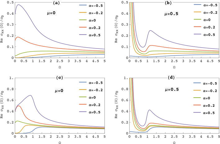
 Γ to X and Y in Figure 3, the energy bands are symmetric but it is not so along the z axis. For α=0, the two subbands touch at Γ making a flat dispersionless band in a small region around it. It is clearly seen that the dispersion around Γ is not linear like that for Dirac or Weyl semimetal. Therefore, we should not expect Dirac or Weyl-like optical conductivity even though two bands just touch at a point. The transverse optical conductivity vanishes because of rotational symmetry of the NLSM. The longitudinal conductivities along different directions are obtained accordingly with the band structure and density of states plots. The anisotropic optical responses of the NLSM are depicted in Figure 5 considering separately two chosen values of μ. The conductivities along x and y are exactly the same. However, along the z direction, the interband contribution for both pristine (μ=0) and the dopped (μ=0.5) NLSM has greater value. The delta peak near Ω=0 is called intraband or Drude conductivity. This peak is formed due to the transition of electrons within the conduction band which we have numerically calculated using the Lorentzian representation for the Dirac δ-function in the expression. For the numerical calculations, we have considered only two low energy bands, and hence the effect of higher energy bands is neglected. The density of states has peak values for some energy range. The conductivity is expected to be minimal for energy greater than that range. The 3D contour bands at low energy in the kx,ky plane are either crossed or gapped depending on the value of kz. When kz=0, two bands cross. However, they open a gap on another plane for kz=0.2. While integrating over the hypercube, the effects from both planes are included which leads to finite values for both interband and intraband conductivity even for pristine NLSM.

Figure 5.

(color online) real part of the longitudinal optical conductivity at T = 0 K measured along the x and z directions in the top to bottom panels, respectively, with (a) and (d) μ=0 and (b) and (c) μ=0.5 for different chosen values of the tuning parameter α. As the value of α is decreased, the conductivity becomes flatter and less dependent on frequency. The given NLSM admits similar responses along x and y and slightly different response along the z direction both quantitatively and qualitatively.

In the case of finite
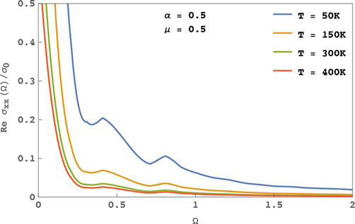
 μ, we have zero conductivity for frequency less than 2μ and a finite jump for frequency greater than 2μ which reveals that the conductivity is due to interband transitions and that transitions obey the Pauli exclusion principle. For photon energy greater than 2μ, the conductivity reaches a maximum value and then is decreased to a minimum saturated value. The peak of the curve depends significantly on the tunable parameter α. The conductivity becomes flat when α goes from positive to negative value. Specifically, the optical conductivity is reduced when a sizable gap is opened by tuning the value of α. Carbotte [22] and Mukherjee [23] have reported the flat conductivity in NLSM with notable finite height. However, our result is more in line with that for ZrSiS [25]. Habe and Koshino illustrated that the optical conductivity of ZrSiS-like NLSM acquires the peak value and then sharply decreases to a flat plateau region and again rises up in the high frequency region. Throughout these calculations, we have considered a toy-model Hamiltonian with only two subbands and small momentum cutoff. Consequently, these results are applicable for small values of chemical potential and for low frequency. For large values of chemical potential and for higher frequency range, the contribution of other subbands to the conductivity may be substantially significant and the conductivity may again increase. The effect due to finite temperature manifests itself through similar qualitative behavior. However, this is quantitatively less responsive compared to that at 0 K. Figure 6 demonstrates that when the temperature is increased from 0 K, the interband optical conductivity is reduced. This is because the thermally excited electrons and holes perturb the optical transition from the valance to the conduction band in the low-frequency regime. Furthermore, when the temperature is increased from room temperature, the separation between the conductivity curves is drastically reduced. This means that the effect due to temperature is more significant in the low-temperature regime.

Figure 6.

(color online) finite temperature response of the optical conductivity measured in the x direction for doped NLSM at α = 0.5. When the temperature is increased from 0 K, the conductivity reduced at low frequency region.

Advertisement

4. Summary and conclusions

In conclusion, we have theoretically investigated the optical responses of nodal-line semimetals using a simple model in conjunction with the Kubo formula for the conductivity. We have derived closed-form semi-analytical expressions for the longitudinal components of the optical conductivity for this simple model whose energy band structure is anisotropic in k-space. Although the model Hamiltonian is simple, the energy band structure still bears similarities to calculated results using the tight-binding model near the Fermi level of a pristine nodal-line semimetal. The effect due to strain is introduced through a parameter α in the model Hamiltonian, thereby making this simple model useful for making qualitative predictions of the NLSM using this heuristic approach. This is bolstered not only by the similarities in the band structure but by the overall qualitative behavior of the conductivity when compared with ZrSiS, for example. We have presented numerical results for the optical conductivity as a function of incident photon energy at both zero and finite temperatures. We analyzed the results considering the effect of strain for the simple model of nodal-line semimetal and chemical potential. We have plotted the band structure along lines joining high-symmetry points in a reduced hypercubic region in kxkykz-space. We emphasize that the model Hamiltonian is particularly representative of the low-energy bands near the Γ point.

The transverse conductivity vanishes due to rotational symmetry around the nodal ring. The Drude conductivity in the limit Ω0 is the result of impurity scattering which is phenomenologically introduced through a Lorentzian representation of the Dirac δ-function with a weak dephasing factor. For charge neutral/pristine NLSM, the interband conductivity is significant near zero frequency. However, for doped NLSM with chemical potential μ0, the interband conductivity rises up to the peak value at Ω=2μ and then decreases. For frequency less than 2μ, Pauli blocking makes electrons unable to make transitions between the valence and conduction bands. At higher photon energies, the transition saturates at its minimum value. This can be explained as a consequence of the cubic Brillouin zone resulting in the value of our wave vector K=kxkykz is restricted to 1ki1 (i=x,y,z), scaled by πa where a is a lattice constant. The Hamiltonian Ĥ, Ω and μ are all scaled in terms of the energy unit υFπ/a. Therefore, the conductivity of NLSM depends on the Fermi velocity υF. The height and width of the peak depend principally on the tuning parameter (α). For α=0, the curve is almost flat at very small transition. At α=0, the bands touch at a point but the quadratic dispersion near Γ is not linear like Dirac or Weyl. Therefore, the conductivity is not flat like that of 2D and 3D Dirac materials as explained in [22, 23, 24]. As we increase the value of α from 0 to larger values, the peak becomes sharper and sharper. In any event, they all converge to a minimum saturated value in the higher frequency region. This is also in agreement with the density of states plot. The density of states has a peak value at a certain energy and zero over a range which could be adjusted by manipulating the value of α. The anisotropic dispersion relations along radial (kx,ky) and axial (kz) directions result in their anisotropic conductivity along these directions. The conductivity along x and y is identical yet the conductivity along z deviates slightly both quantitatively and qualitatively. The anisotropic conductivities in Shahin’s [24] paper are explained as a consequence of an anisotropic Fermi surface where they have considered the toroidal shape. These properties indicate possible applications involving microelectronics technologies, integrated circuits and devices, ultrafast modulators and high performance transistors.

We have also calculated the finite temperature-dependent response of the interband conductivity. Although the temperature suppresses transitions between subbands and reduces the conductivity, there is still qualitative similarity between the behavior of the response for the model Hamiltonian adapted here and that derived with the use of the tight-binding model. Therefore, the overall response of the optical conductivity for the chosen model Hamiltonian is suitable for investigating NLSM rather than that of Dirac or Weyl semimetals. The cubic Brillouin zone and the band structure plots suggest that the dispersion relations of our model Hamiltonian is more or less appropriate for drawing comparisons with that of ZrSiS. As a matter of fact, a few years ago, the dynamical optical conductivity of ZrSiS was investigated using a multi-orbital tight-binding model based on the first-principles band calculation [25] which agrees with our results that the optical conductivity of some TNLSM are significantly divergent from Dirac and Weyl semimetals. The reduced conductivity in the high frequency region was not fully explored in previous similar studies. While analyzing our results, we should not forget that we have considered the low energy, low-band model Hamiltonian. Therefore, the results would not be reliable for very high chemical potential and very high photon energies. In the higher frequency region, the effect of other bands and the higher order terms in the wave vector may not be negligible. This may result in substantial effect on the obtained optical conductivity. Finally, we came to the conclusion that different nodal-line semimetals described by specific model Hamiltonians may not have the same optical response in chosen frequency regions. The model Hamiltonian we considered has ZrSiS like dispersion relation and the conductivity also mimics well qualitatively with the overall behavior and this is encouraging to investigate the self-sustained charge density oscillations, i.e., plasmons.

Advertisement

Acknowledgments

G.G. would like to acknowledge the support from the Air Force Research Laboratory (AFRL) through Grant No. FA9453-21-1-0046. We would like to thank Dr. Po-Hsin Shih for helpful discussions and guidance on the numerical calculations and interpretation of the results.

References

  1. 1. Lv BQ, Qian T, Ding H. Experimental perspective on three-dimensional topological semimetals. Reviews of Modern Physics. 2021;93:025002
  2. 2. Muechler L, Topp A, Queiroz R, Krivenkov M, Varykhalov A, Cano J, et al. Modular arithmetic with nodal lines: Drumhead surface states in ZrSiTe. Physical Review X. 2020;10:011026
  3. 3. Pan H, Tong B, Jihai Y, Wang J, Dongzhi F, Zhang S, et al. Three-dimensional anisotropic magnetoresistance in the Dirac node-line material ZrSiSe. Scientific Reports. 2018;8:9340. DOI: 10.1038/s41598-018-27148-z
  4. 4. Yinming Shao AN, Rudenko JH, Sun Z, Zhu Y, Seongphill Moon AJ, Millis SY, et al. Electronic correlations in nodal-line semimetals. Nature Physics. 2020;16:636
  5. 5. Murakami S. Phase transition between the quantum spin hall and insulator phases in 3D: Emergence of a topological gapless phase. New Journal of Physics. 2007;9:356
  6. 6. Wang Z, Sun Y, Chen X-Q, et al. Dirac semimetal and topological phase transitions in a3 Bi (a=N, K, Rb). Physical Review B. 2012;85:195320
  7. 7. Burkov A, Hook M, Balents L. Topological nodal semimetals. Physical Review B. 2011;84:235126
  8. 8. Yang M-X, Luo W, Chen W. Quantum transport in topological nodal-line semimetals. Advances in Physics X. 2022;7:2065216
  9. 9. Fang C, Chen Y, Kee H-Y, Fu L. Topological nodal line semimetals with and without spin-orbital coupling. Physical Review B. 2015;92:081201(R)
  10. 10. Hosen MM, Dhakal G, Wang B, Poudel N, Dimitri K, Kabir F, et al. Experimental observation of drumhead surface states in SrAs3. Scientific Reports. 2020;10:2776
  11. 11. Wang X, Ding G, Cheng Z, Surucu G, Wang X-L, Yang T. Novel topological nodal lines and exotic drum-head-like surface states in synthesized CsCl-type binary alloy TiOs. Journal of Advanced Research. 2020;22:137
  12. 12. Li S, Yu Z-M, Liu Y, Guan S, Wang S-S, Zhang X, et al. Type-II nodal loops: Theory and material realization. Physical Review B. 2017;96:081106
  13. 13. Bian G, Chang T-R, Zheng H, Velury S, Xu S-Y, Neupert T, et al. Drumhead surface states and topological nodal-line fermions in TiTaSe2. Physical Review B. 2016;93:121113
  14. 14. Weng H, Liang Y, Xu Q, Yu R, Fang Z, Dai X, et al. Topological node-line semimetal in three-dimensional graphene networks. Physical Review B. 2015;92:045108
  15. 15. Neupane M, Belopolski I, Hosen MM, et al. Observation of topological nodal fermion semimetal phase in ZrSiS. Physical Review B. 2016;93:201104
  16. 16. Topp A, Lippmann JM, Varykhalov A, et al. Non-symmorphic band degeneracy at the Fermi level in ZrSiTe. New Journal of Physics. 2016;18:125014
  17. 17. Zhao J, Yu R, Weng H, et al. Topological node-line semimetal in compressed black phosphorus. Physical Review B. 2016;94:195104
  18. 18. Xu G, Weng H, Wang Z, et al. Chern semimetal and the quantized anomalous hall effect in HgCr2Se4. Physical Review Letters. 2011;107:186806
  19. 19. Nicol EJ, Carbotte JP. Optical conductivity of bilayer graphene with and without an asymmetry gap. Physical Review B. 2008;77:155409
  20. 20. Fang C, Weng H, Dai X, Fang Z. Topological nodal line semimetals. Chinese Physics B. 2016;25:117106
  21. 21. Zhou W, Rudenko AN, Yuan S. Effect of mechanical strain on the optical properties of nodal-line semimetal ZrSiS. Advanced Electronic Materials. 2020;6(1):1900860
  22. 22. Carbotte JP. Optical response of a line node semimetal. Journal of Physics. Condensed Matter. 2017;29:045301
  23. 23. Mukherjee SP, Carbotte JP. Transport and optics at the node in a nodal loop semimetal. Physical Review B. 2017;95:214203
  24. 24. Barati S, Abedinpour SH. Optical conductivity of three and two dimensional topological nodal line semimetals. Physical Review B. 2017;96:155150
  25. 25. Habe T, Koshino M. Dynamical conductivity in the topological nodal-line semimetal ZrSiS. Physical Review B. 2018;98:125201
  26. 26. Wang C, Wen-Hui X, Zhu C-Y, Chen J-N, Zhou Y-L, Deng M-X, et al. Anomalous hall optical conductivity in tilted topological nodal-line semimetals. Physical Review B. 2021;103:165104
  27. 27. Chan Y-H, Ching-Kai Chiu MY, Chou and Andreas P. Schnyder. Ca3P2 and other topological semimetals with line nodes and drumhead surface states. Physical Review B. 2016;93:205132
  28. 28. Nag T, Menon A, Basu B. Thermoelectric transport properties of Floquet multi-Weyl semimetals. Physical Review B. 2020;102:014307
  29. 29. Tabert C, J. Electronic Phenomena in 2D Dirac-Like Systems: Silicene and Topological Insulator Surface States. Guelph, Canada: The University of Guelph; 2015

Written By

Sita Kandel, Godfrey Gumbs and Oleg L. Berman

Submitted: 24 January 2023 Reviewed: 13 March 2023 Published: 28 June 2023