
Abstract
This chapter mainly enlighten about the development and trends of the field effect transistors (FETs) in the nanoelectronics industries. According to Moore’s law, the number of transistors doubles in every 2 years because of transistor’s size is scaled down. Though the scaling of MOSFET has been the driving force towards the technological advancement, but due to continuous scaling various secondary effect which include; short channel effects, high leakage current, excessive process variation and reliability issue degrades the device performance. In today’s era, researchers are developing nano scaled transistors using various types of materials with different device geometries to reduce the limitations of conventional MOSFET. This chapter focuses on the development history, current-status and future trends of transistors. At the same time, the various protentional applications of nano-transistor discussed in this chapter.
Keywords
- short channel effects
- transistor miniaturization
- gate-all- structure
- field effect transistors
- nanoelectronics
1. Introduction
In the ever-evolving landscape of semiconductor technology, the Metal-Oxide-Semiconductor Field-Effect-Transistors (MOSFETs) stands as a cornerstone, constantly evolving to meet the demands of modern electronic (Nano electronics) and shaping the future of the electronic devices. Gordon Moore, co-founder of INTEL, states that the number of transistors on a microchip double approximately every 2 years, leading to an exponential increase in computing power [1, 2]. The essence of Moore’s law is the relentless miniaturization of transistors, allowing for more computing power in smaller spaces and at lower costs. This trend has led to the development of increasingly powerful and energy-efficient electronic devices, which are fundamental to the growth of the digital revolution.
This chapter delves into the dynamic realm of MOSFETs, exploring the latest advancements that define the present and peering into the exciting possibilities that lie ahead. As we embark on a journey through the cutting-edge developments and emerging trends, we unravel the MOSFETs on the horizon, shedding light on the innovations that promise to revolutionize the world of electronics. In this chapter we also navigate the current progress, uncovering what’s new and contemplating the boundless potentials that awaits in the realm of MOSFET technology.
2. Development history of transistor
Figure 1 illustrates the evolution of the transistor technology. In 1947, the First working transistor (point contact transistor) was invented by John Bardeen, Walter Brattain and William Shockley at Bell Laboratory [3]. Shockley unveiled an enhanced iteration of the point contact transistor, known as the bipolar junction transistor (BJT), in 1948 [4]. This enhanced iteration, formally put into production in the early 1950s, marked a pivotal juncture that initiated the widespread adoption of transistors.
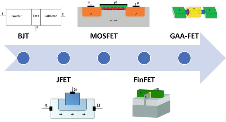
Figure 1.
Evolution of transistor.
While the BJT brought about significant advancements, it also presented its own set of advantages and limitations. To address challenges such as low thermal stability, substantial noise and slow switching speeds, researchers sought the next evolution in transistor technology. Following the conceptualization of the Field Effect Transistor (FET) by J. E. Lilienfeld in 1925 [5], the first junction field effect transistor (JFET) was presented by Henrich Welker in 1945 [6]. Subsequently, in 1959, Mohamed Atalla and Dawon Kahng pioneered the silicon metal oxide semiconductor field effect transistor (Si-MOSFET) [7]. This marked a crucial milestone in transistor development, introducing a new paradigm with enhanced performance characteristics.
2.1 Bipolar junction transistor
As shown in Figure 1, Bipolar Junction Transistor (BJT) is a three-terminal semiconductor based current control device, which has emitter, base, and collector terminals. The main function of transistor is to control the flow of current between emitter and collector by using base terminal. Generally, the emitter current (IE) is the sum of base current (IB) and the collector current (IC) [8].
Due to the limitations of the BJT as low thermal stability, low switching speed and high noise, researchers were looking into new electronic device [9, 10].
2.2 Junction field effect transistors
Junction Field Effect Transistor (JFET) functions as a voltage-controlled transistor, characterized as a unipolar device featuring three terminals- source, drain and gate. The gate serves the purpose of regulating the output voltage. In contrast to Bipolar Junction Transistor (BJT), JFET exhibits superior attributes such as heightened thermal stability, reduced noise and compact size. However, its limitations in handling low signals paved the way for the emergence of Metal-Oxide-Semiconductor Field-Effect Transistor (MOSFET) [11, 12].
2.3 Metal-oxide semiconductor field effect transistor
MOSFET is another type of filed effect transistor which has a metal oxide semiconductor (MOS) structure. Similar to JFET, MOSFET has three terminals (source, drain and gate) which are used to control the conductivity between source and drain terminal based on the applied gate voltage. Based on the Moore’s law, while the scaling of MOSFET has been the primary catalyst for technological advancement, the relentless scaling has given rise to several ancillary effects. These effects encompass short channel phenomena, increased leakage current, drain induced barrier lowering, and concerns related to device reliability, all of which collectively compromise the overall performance of the device [13, 14, 15]. The limitations associated with attempting to scale down traditional semiconductor devices have led researchers to look into the following possible solutions [16, 17, 18]:
Alter the prevailing FET structure
Employ a novel material as a substitute for silicon as the channel/substrate
Utilization of materials with a high relative dielectric constant (εr, high for gate application
2.4 Fin field effect transistor
As shown in Figure 1, Fin FET is the three-dimension structure of a transistor. Instead of a flat channel, it features a fin like structure that rise above the substrate, providing better control over the flow of current. FinFET technology is commonly used in modern semiconductor manufacturing process, offering improved performance and energy efficiency compare to traditional transistors [19, 20]. It serves as the foundation for contemporary nanoelectronic semiconductor device manufacturing.
2.5 Gate-all-around field effect transistor
Gate-All-Around Field Effect Transistor (GAA-FET) is a type of transistor design where the gate material completely surrounds the channel region from all sides, providing better control over the flow of current. GAA-FET emerges as a promising advancement in semiconductor manufacturing, addressing scaling and performance limitations inherent in traditional transistor design [21]. This innovative architecture enables enhanced electrostatic control and mitigate leakage, surpassing the constraints of conventional transistor configurations [22].
3. Scaling
According to Moore, the principle of scaling involves increasing the density of transistor per unit volume on a singular integrated chip. Figure 2 illustrates the scaled-down dimensions of the transistor across various technology nodes in semiconductor devices. Notably, the gate length is projected to reduce to approximately 3 nm by 2024 [23, 24]. The scaling of the Field Effect Transistors has been a driving catalyst for the progression of the nano-electronic devices. Nevertheless, persistent scaling introduces challenges such as short channel effects (including source/drain charge sharing, drain-induced barrier lowering, surface punchtrough, mobility degradation and velocity saturation) and heightened in leakage current [25, 26, 27].
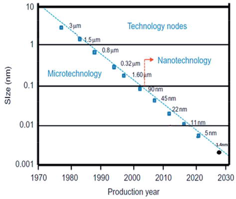
Figure 2.
Technology node roadmap for transistors.
The reduction in transistor size also leads to a decrease in oxide thickness, contributing to an escalation in gate leakage current. Consequently, for nano-scale design, the minimization of leakage power becomes equally imperative. The complications associated with scaling down traditional MOSFET prompted researchers to explore Gate-all-around structure-based transistors or nanotransistors. These novel transistors have undergone extensive scrutiny for diverse applications such as logic devices, memory devices, sensors etc. However, accurately predicting the ultimate performance of these innovative nanotransistors remain a challenge. To provide valuable insights, guide development efforts, and reduce costs, the development of precise and reliable simulation tools emerges as a paramount concern.
4. Nanotransistors
Semiconductor microelectronics has now transitioned into a genuine nano-electronic technology. Nanotechnology, defined by structures with at least two dimensions below 100 nm, material properties influenced by size and structures involving self-assembly, finds a perfect fit in silicon nanoelectronics [28, 29]. Semiconductor nanoelectronics full-fills all three criteria and can be recognized as the inaugural instance of active nanotechnology in manufacturing. As silicon technology undergoes the shift to nanoelectronics, a novel realm of research has emerged. Unconventional nanoelectronics leverages semiconductor nanotubes and nanowires, while molecular electronics employs molecules as electronic devices. The trajectory of this research towards practical electronic technologies remains uncertain, but its impact on practical nanoelectronics is evident in at least three aspects. Firstly, there is the development of new techniques for assembling nanostructures materials and nanoscale. Secondly, there is the advancement of novel methods for assembling nanostructured materials and nanoscale devices. Thirdly, there is a discernible comprehension of electronic devices at the nanoscale, called nanotransistors.
A transistor whose dimensions are in nanometers, called nanotransistor. Figure 3 [30] shows the structure of nano-transistor. It is a compact and efficient electronic device and often associated with advancement in nanoelectronics and nanotechnology. The development of the nanotransistors is crucial for keeping up with Moore’s Law, which trends has driven the miniaturization of electronic components, leading to more powerful and energy-efficient devices.
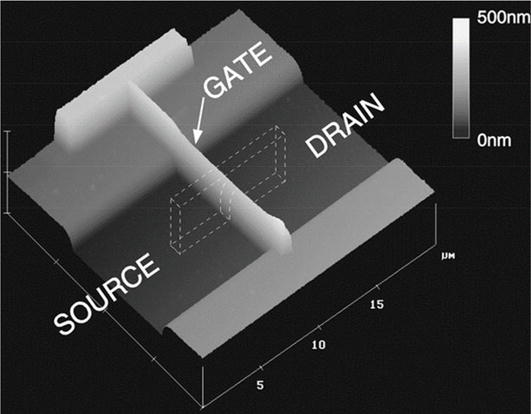
Figure 3.
A 3-D atomic force microscopic view of nanotransistor [
5. Applications
MOSFET find widespread applications across various electronic devices and systems due to their versatile and controllable nature. Some key applications are as follows (Figure 4) [31, 32, 33, 34, 35, 36, 37, 38, 39, 40, 41]:
Amplifiers: FETs are commonly used as amplifiers in electronics circuits. They can amplify signal with low distortion and noise, making them suitable for applications in audio amplifiers, radio frequency (RF) amplifiers and another signal processing circuits.Switching Circuits: FETs can operate as electronic switches in digital circuits. MOSFETs, are extensively used in digital integrated circuits, such as CMOS (complementary Metal-Oxide-Semiconductor) technology.Voltage-Controlled Oscillators (VCOs): FETS can be used in voltag-controlled oscillators to generate variable frequency signals. This is useful in applications such as frequency modulation (FM) communication systems.Mixers and Modulators: FETs are employed in mixer circuits used in RF and communication systems. They are also used in modulator circuits to modulate signals for various communication applications.Low-Noise Preamplifiers: Due to their low noise characteristics, FETs are often used in the front-end of sensitive electronic systems, such as in low-noise amplifiers for communication receivers.Voltage Regulators: FETs are used in voltage regulator circuits to regulate and stabilize the output voltage of power supplies.Integrated circuits (ICs): FETs are fundamental component in the design of integrated circuits. Including microprocessors, memory chips and other digital and analog ICs.Sensors: MOSFETs can be utilized as sensors in various application due to their sensitivity to change in certain physical quantities. Here are some ways in which MOSFETs are employed as sensors.Gas Sensors: MOSFETs can be used as gas sensors by incorporating a sensing material on the gate oxide. When exposed to specific gases, the electrical properties of the MOSFET change, leading to a measurable variation in the output current or voltage. This is commonly employed in gas detection systems.Chemical Sensors: MOSFETs can be serve as chemical sensors by modifying the gate oxide with a material that interacts with specific chemicals. Changes in the chemical environment result in a shift in the electrical characteristics of the MOSFET, allowing for the detection of a particular chemical compounds.Biological Sensors: MOSFETs modified with biomolecules or biological receptors can be used for sensing biological entities such as DNA, protein, or other biomolecules. The binding of target biomolecules to the modified MOSFET surface induced changes in the transistor’s electrical properties, enabling the detection of biological interactions.pH Sensors: MOSFET can be configured as pH sensors by modifying the gate oxide with materials sensitive to change in pH levels. Variations in the pH of the surrounding environment result in changes in the MOSFET’s threshold voltage or conductance, providing a means for pH measurement.Temperature Sensors: MOSFETs can be used as temperature sensors by exploiting the temperature-dependent characteristics of the transistor. Changes in temperature affect the MOSFET’s threshold voltage and mobility, allowing it to function as a temperature-sensitive device.Radiation Sensors: MOSFETs can be sensitive to ionizing radiation. By using specially designed MOSFETs. They can be employed as radiation sensors in applications such as dosimetry and radiation monitoring.Pressure Sensors: MOSFETs can be integrated into pressure sensor devices by incorporating a flexible diaphragm that mechanically affects the transistor’s electrical characteristics in response to change in pressure.Light Sensors: MOSFETs can be employed in light sensors or photodetector by utilizing their sensitivity to light. Light falling on the MOSFET’s surface generates charge carriers, affecting the transistor’s conductivity. This is used in applications such as ambient light sensors in electronic devices.Humidity Sensors: The electrical properties of MOSFET can be influenced by humidity changes. Modified gate oxide can be employed to make MOSFETs responsive to variations in humidity levels, making them suitable for humidity sensing applications.Utilizing MOSFETs as sensors provides advantages such as high sensitivity, miniaturization potential, and compatibility with integrated circuit technology. These properties make them suitable for a wide range of sensing applications in diverse fields.
Charges-Coupled Devices (CCDs): MOSFETs are commonly used in the construction of CCDs, which are essential in imaging devices such as digital cameras and camcorders.Biomedical Devices: FETs find applications in biomedical devices, such as biosensors and neural interfaces, where their electrical properties make them suitable for interfacing with biomedical systems.
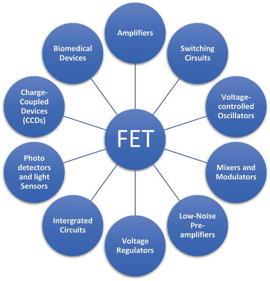
Figure 4.
Applications of field effect transistors [
These applications showcase the versatility of FETs in a wide range of electronic devices and systems across different industries.
6. Conclusion
This chapter offers a comprehensive review of transistors, encapsulating their evolutionary journey through four key perspectives: (1) the historical development of transistors, (2) constraints arising from scaling, (3) nanotransistors, and (4) contemporary and prospective applications shaping the present and future landscape of transistor utilization. In the realm of semiconductor technology, FET play a pivotal role, continuous evolving to meet the demands of modern electronics. This chapter explores the dynamic history of transistors, from the groundbreaking point contact transistor to the evolution of BJT, JFET, and the transformative MOSFET. The discussion encompasses limitations and solutions, including the introduction of FinFET and the promising potential of GAA-FET in overcoming scaling challenges.
While emphasizing the driving force of scaling in technological process, the chapter acknowledges the associated challenges like short channel effects and increased leakage current. Researchers are actively exploring alternative solutions, including alternating FET structures and materials. The exploring extends into the realm of nanotransistors, emphasizing their importance in the era of nanoelectronics and their critical role in sustain Moore’s Law.
Lastly, the extensive applications of FET across diverse domains underscore their versatility in amplifiers, switching circuits, sensors and biomedical devices. The constant innovation and adaption in MOSFET technology are recognized as shaping the future of electronics, promising continued breakthroughs and advancements in the field.
References
- 1.
Shalf J. The future of computing beyond Moore’s Law. Philosophical Transactions of the Royal Society A. 2020; 378 :20190061 - 2.
Thompson SE, Parthasarathy S. Moore's law: The future of Si microelectronics. Materials Today. 2006; 9 :20-25 - 3.
Hasegawa S, Grey F. Electronic transport at semiconductor surfaces––From point-contact transistor to micro-four-point probes. Surface Science. 2002; 500 :84-104 - 4.
Bondyopadhyay PK. The beginning junction transistor. Proceedings of the IEEE. 1998; 86 :63-77 - 5.
Ragavendran U, Ramachandran M. Low power and low area junction-less tunnel FET design. International Journal of Engineering & Technology. 2018; 7 :155-157 - 6.
Choi YC, Cha H-Y, Eastman LF, Michael G. Spencer: A new 4H-SiC normally off lateral channel vertical JFET with extremely low power losses: Source inserted double-gate structure with a supplementary highly doped region. IEEE Transactions on Electron Devices. 2005; 52 :1940-1948 - 7.
Rafin SMS, Hossain RA, Haque MA, Hossain MK, Haque MA, Mohammed OA. Power electronics revolutionized: A comprehensive analysis of emerging wide and ultrawide bandgap devices. Micromachines. 2023; 14 :2045 - 8.
Sahu A, Bramhane LK, Singh J. Symmetric lateral doping-free BJT: A novel design for mixed signal applications. IEEE Transactions on Electron Devices. 2016; 63 :2684-2690 - 9.
Nenadovic N, Nanver LK, Slotboom JW. Electrothermal limitations on the current density of high-frequency bipolar transistors. IEEE Transactions on Electron Devices. 2004; 51 :2175-2180 - 10.
Chen C, Labrousse D, Lefebvre S, Petit M, Buttay C, Morel H. Study of short-circuit robustness of SiC MOSFETs, analysis of the failure modes and comparison with BJTs. Microelectronics Reliability. 2015; 55 :1708-1713 - 11.
Levinzon FA. Noise of the JFET amplifier. IEEE Transactions on Circuits and Systems I: Fundamental Theory and Applications. 2000; 47 :981-985 - 12.
Baertsch RD, Engeler WE, Goldberg HS, Puckette CM. Fully integrated analog filters using bipolar-JFET technology. IEEE Journal of Solid-State Circuits. 1978; 13 :814-821 - 13.
Khanna VK. Short-channel Effects in MOSFETs: Integrated Nanoelectronics. New Delhi: Springer; 2016. pp. 73-93 - 14.
Kumar MJ. Controlling short-channel effects in deep-submicron SOI MOSFETs for improved reliability: A review. IEEE Transactions on Device and Materials Reliability. 2010; 4 :99-109 - 15.
D’Agostino F, Quercia D. Short-channel effects in MOSFETs. Introduction to VLSI Design (EECS 467). 2000; 70 :71-72 - 16.
Huq SI, Nafreen M, Rahman T, Bhadra S. Comparative study of full adder circuit with 32nm MOSFET, DG-FinFET and CNTFET. In: 4th International Conference on Advances in Electrical Engineering (ICAEE). Dhaka; 2017. pp. 38-43 - 17.
Wu M, Alivov YI, Morkoc H. High-κ dielectrics and advanced channel concepts for Si MOSFET. Journal of Materials Science: Materials in Electronics. 2008; 19 :915-951 - 18.
Long W, Ou H, Kuo JM, Chin KK. Dual-material gate (DMG) field effect transistor. IEEE Transactions on Electron Devices. 1999; 4 :865-870 - 19.
Hisamoto D et al. FinFET-a self-aligned double-gate MOSFET scalable to 20 nm. IEEE Transactions on Electron Devices. 2000; 47 :2320-2325 - 20.
Dixit A, Gupta N. A compact model of gate capacitance in ballistic gate-all-around carbon nanotube field effect transistors. International Journal of Engineering. 2021; 34 :1718-1724 - 21.
Das UK, Bhattacharyya TK. Opportunities in device scaling for 3-nm node and beyond: FinFET versus GAA-FET versus UFET. IEEE Transactions on Electron Devices. 2020; 67 :2633-2638 - 22.
Cutress I. Intel’s Manufacturing Roadmap from 2019 to 2029: Back Porting, 7 nm, 5 nm, 3 nm, 2 nm, and 1.4 nm. AnandTech; 11 Dec 2019 - 23.
Das UK, Bhattacharyya TK. Opportunities in device scaling for 3-nm node and beyond: FinFET versus GAA-FET versus UFET. IEEE Transactions on Electron Devices. 2020; 67 :2633-2638 - 24.
Devi D, Rakesh P, Rakesh V. Impact of scaling gate insulator thickness on the performance of carbon nanotube field effect transistors (CNTFETs). Journal of Nano-and Electronic Physics. 2013; 5 :02014-02019 - 25.
Yu L, Chang S, Ahmed H, Wang S, Bell CY, Yang C, et al. FinFET scaling to 10 nm gate length. In: Digest International Electron Devices Meeting. San Francisco, USA; 2002. pp. 251-254 - 26.
Gupta N, Dixit A. Carbon Nanotube Field-Effect Transistors (CNFETs): Structure, Fabrication, Modeling, and Performance. Carbon Nanomaterial Electronics: Devices and Applications. Singapore: Springer Singapore; 2021. pp. 199-214 - 27.
Lundstrom MS. Fundamentals of Nanotransistors. Vol. 6. Indiana, USA: World Scientific Publishing Company; 2016 - 28.
Li J, Li Y, Zhou N, Xiong W, Wang G, Zhang Q , et al. Study of silicon nitride inner spacer formation in process of gate-all-around nano-transistors. Nanomaterials. 2020; 10 :793 - 29.
Timp G, Bude J, Bourdelle KK, Garno J, Ghetti A, Gossmann H, et al. The ballistic nano-transistor. In: International Electron Devices Meeting. USA; 1999. pp. 55-58 - 30.
Singh S et al. Implementation of gate-all-around gate-engineered charge plasma nanowire FET-based common source amplifier. Micromachines. 2023; 14 :1357 - 31.
Yim S-M, Kk O. Switched resonators and their applications in a dual-band monolithic CMOS LC-tuned VCO. IEEE Transactions on Microwave Theory and Techniques. 2006; 54 :74-81 - 32.
Nouri R, Guan W. Nanofluidic charged-coupled devices for controlled DNA transport and separation. Nanotechnology. 2021; 32 :345501 - 33.
Sreenivasulu V, Narendar V. Design and temperature assessment of junctionless nanosheet FET for nanoscale applications. Silicon. 2022; 14 :3823-3834 - 34.
Mishra AK, Jarwal DK, Mukherjee B, Kumar A, Ratan S, Jit S. CuO nanowire-based extended-gate field-effect-transistor (FET) for pH sensing and enzyme-free/receptor-free glucose sensing applications. IEEE Sensors Journal. 2020; 20 :5039-5047 - 35.
Dixit A, Gupta N, Chaturvedi N. Ab initio study of carbon nanotube field effect transistor gas sensor for detection of Ammonia and nitrogen dioxide gas. IEEE Transactions on Nanotechnology. 2022; 21 :564-574 - 36.
Tiwari S, Saha R. Improved optical performance in near visible light detection photosensor based on TFET. Microelectronics Journal. 2022; 129 :105554 - 37.
Sedki M, Shen Y, Mulchandani A. Nano-FET-enabled biosensors: Materials perspective and recent advances in North America. Biosensors and Bioelectronics. 2021; 176 :112941 - 38.
Li H, Li D, Chen H, Yue X, Fan K, Dong L, et al. Application of silicon nanowire field effect transistor (SiNW-FET) biosensor with high sensitivity. Sensors. 2023; 23 :6808 - 39.
Mishra AK, Jarwal DK, Mukherjee B, Kumar A, Ratan S, Jit S. CuO nanowire-based extended-gate field-effect-transistor (FET) for pH sensing and enzyme-free/receptor-free glucose sensing applications. IEEE Sensors Journal. 2020; 20 :5039-5047 - 40.
Dai C, Liu Y, Wei D. Two-dimensional field-effect transistor sensors: The road toward commercialization. Chemical Reviews. 2022; 122 :10319-10392 - 41.
Gelao G, Marani R, Perri AG. Effect of CNT parameters variations on CNTFET amplifier performance. ECS Journal of Solid State Science and Technology. 2023; 12 :011004