Open Access is an initiative that aims to make scientific research freely available to all. To date our community has made over 100 million downloads. It’s based on principles of collaboration, unobstructed discovery, and, most importantly, scientific progression. As PhD students, we found it difficult to access the research we needed, so we decided to create a new Open Access publisher that levels the playing field for scientists across the world. How? By making research easy to access, and puts the academic needs of the researchers before the business interests of publishers.
We are a community of more than 103,000 authors and editors from 3,291 institutions spanning 160 countries, including Nobel Prize winners and some of the world’s most-cited researchers. Publishing on IntechOpen allows authors to earn citations and find new collaborators, meaning more people see your work not only from your own field of study, but from other related fields too.
Resistive RAM (RRAM) synaptic plasticity behavior is essential to enable future power-efficient brain-inspired accelerators. In oxide-based RAM (so-called OxRAM), synaptic plasticity is reflected in the OxRAM conductance modulation capability, making the technology well suited for neuromorphic applications. This chapter assesses the conductance modulation of HfO2-based RRAM and leverages experimental measurement results to establish the inherent synaptic behavior of the technology. The OxRAM conductance modulation capability is demonstrated based on a 1T1R elementary memory array test chip. The memory array OxRAM cells are operated using two distinct programming schemes. The first one is based on RESET (RST) peak voltage modulation. The second one is based on SET compliance current modulation. Both methods show that OxRAM conductance modulation is highly impacted by the variability of the technology. Hence, variability happens to be one the most challenging limitations for OxRAMs used in neuromorphic applications.
M2NP, UMR CNRS 7334, Aix-Marseille Université, Marseille, France
*Address all correspondence to: hassen.aziza@univ-amu.fr
1. Introduction
The significant growth in portable and connected devices constantly produces a huge volume of data [1]. At the same time, edge-Artificial Intelligence (AI) applications, which require processing and storage of data in close vicinity [2], accelerate the demand for more memory space. In the last 20 years, different memory concepts have been explored, aiming to mitigate the major limitations of existing solid-state memories: the volatility of RAM technology and the high latency of Flash [3]. In this context, Resistive RAM (RRAM), with its simple structure, low latency (∼10 ns), small size (<10 nm), compatibility with current CMOS manufacturing processes, and low power operation, is believed to be the best contender [4].
At the system level, conventional computing technology based on the Von Neumann (VN) architecture is facing fundamental limits such as low energy efficiency and latency [5]. It results in the development of alternative information processing architectures categorized as non-Von Neumann (non-VN) [6]. To date, there has been a lot of research activities dedicated to the development of bio-inspired computing architectures such as Artificial Neuromorphic Networks (ANNs) [7]. Indeed, ANNs have demonstrated better performances in identification tasks compared to VN hardware architectures. ANNs are meant to mimic biological neuromorphic networks. They are based on units, referred to as neurons, that are connected in specific patterns. A synapse, associated with a weight, acts as a “programmable” link between each neuron. Weights generally stimulate or attenuate the signal passing through the network [8].
RRAM devices [9, 10] are seen as the optimal candidates to mimic biological synapses as they possess the capability to modulate their conductance [11, 12]. Among all the alternative RRAM technologies, OxRAMs have proven to be very effective in implementing some aspects of synaptic plasticity [13, 14]. Synaptic plasticity in OxRAMs relies on the MultiLevel Cell (MLC) storage capability of the technology, which has been reported in many studies related to neuromorphic applications [15, 16, 17]. During a SET programming operation, MLC can be applied to the OxRAM by modulating its compliance current. During an RST operation, MLC can be obtained by varying the RST voltage level. Another technique consisting in varying the pulse widths and amplitudes during SET or RST operations can also be used. However, in most prior works, MLC operation has been implemented at the device level, and MLC implementation at the circuit and system levels remains to be explored [18, 19, 20]. Also, and more importantly, RRAM variability poses a significant hurdle for RRAM widespread adoption in neuromorphic computing systems. Variability refers to the inherent differences in the electrical characteristics of RRAM devices, even when fabricated under the same manufacturing conditions. This variability can manifest as variations in key parameters of RRAM devices including the resistance levels, thus preventing reliable and predictable device behavior, which is crucial for accurate neural network operations [21].
In this chapter, we present how OxRAM memory devices can be used for synaptic plasticity functions. The conductance modulation of the OxRAM cell is demonstrated versus variability at a memory array test chip level by modulating the peak voltage applied to the cell during an RST operation or by modulating the current passing through the cell during a SET operation. This chapter is organized as follows. Section II presents the OxRAM technology along with memristor-based neuromorphic networks’ basic concepts. In Section III, the conductance modulation capability of the OxRAM technology is evaluated experimentally versus variability using a dedicated test chip. In Section IV, the conductance modulation capability of OxRAM is discussed. Finally, Section V concludes the paper.
2. Background: RRAM technology for neuromemristive systems
2.1 OxRAM technology
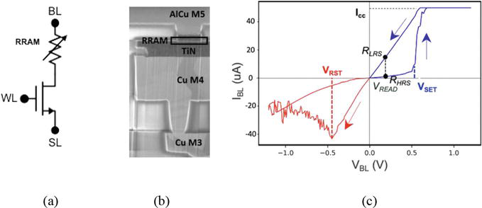
Figure 1a shows a 1T1R OxRAM cell with one MOS transistor connected serially with the resistive element. The resistive element, presented in Figure 1b, is integrated in the back end of line (BEOL) of a 130 nm conventional CMOS technology, between the two last metal levels (Metal 4 and Metal 5) [22]. Layers composing the resistive element are deposited on the substrate surface by means of physical vapor deposition where a 10 nm Hafnium dioxide (HfO2) thin film is placed on top of a TiN Bottom electrode (BE). A Ti/TiN stack is then added to form the top electrode (TE). A typical 1T1R I-V hysteresis is presented in Figure 1c. According to this hysteresis, the OxRAM can be operated as follows: after a preliminary forming (FMG) step [23], the memory cell can be switched reversibly between two resistance states, the Low Resistance State (LRS) and the High Resistance State (HRS). The switching mechanism is characterized by a sudden change in the cell current. The current change is triggered by biasing the 1T1R cell with specific voltages, VSET to switch from HRS to LRS during a SET operation and VRST to switch from LRS to HRS during an RST operation.
Figure 1.
(a) Symbol view of a 1T1R RRAM cell. (b) SEM cross section of the RRAM cell [20] and (c) OxRAM I–V hysteresis.
FMG, RST, SET, and read bias voltages are given in Table 1, with the corresponding nominal resistance levels. The read operation, used to sense the memory cell state, can be performed non-destructively. Typically, a small read voltage (around 0.1 V) is used to not disturb the current state of the cell. This allows for read operations to be performed frequently without affecting the reliability of the device. RHRS and RLRS levels are extracted in the forward or SET direction (blue curve in Figure 1c, with VBL > 0). In practice, at the circuit level, the read operation is performed by measuring the current associated with the RLRS and RHRS resistances to determine whether the cell is in logic ‘0’ (HRS) or the logic ‘1’ (LRS). In the 1T1R cell architecture, the amount of current passing through the cell is controlled according to the select transistor gate voltage bias. This maximal current or clamping current is referred to as ICC. From a reliability and functionality standpoint, it has been demonstrated that one of the most important limitations of OxRAM technology is related to the memory cell variability (spatial and temporal) [24, 25]. Actually, variability in RHRS/RLRS is so erratic that the technology has been employed as an entropy source in True Random Number Generators (TRNG) [26, 27].
FMG
RST
SET
Read
WL
2 V
2.5 V
2 V
2.5 V
BL
3.3 V
0 V
1.2 V
0.1 V
SL
0 V
1.2 V
0 V
0 V
RLRS/HRS
10 kΩ
240 kΩ
15 kΩ
—
Table 1.
OxRAM cell standard operating voltages.
2.2 OxRAM as a synapse
Synapses are central elements in biological neuromorphic networks; however, a basic electronic device emulating synapses is not available yet, thus complicating the development of integrated circuits able to mimics biological systems [28]. OxRAMs have shown the ability to be used as synapses within hybrid CMOS-memristive devices [29, 30]. Actually, the OxRAM cell has been identified as a possible candidate for building an electronic equivalent of a biological synapse as its conductance can be electrically increased or decreased [31]. In neuromorphic network architectures, OxRAM devices are meant to store synaptic weights. Furthermore, OxRAM technology can be integrated within crossbar and 3D architectures to reach integration densities never seen before [32].
Although the potential of OxRAM to mimic the synaptic behavior has been demonstrated in many studies [28], OxRAM neuromorphic network architectures also have some limitations that have been pointed out in the literature. Here are a few commonly mentioned limitations. Crossbar arrays leverage the non-linear relationship between the voltage and resistance of particular RRAM devices, which is essential to avoid the integration of the select transistor. Avoiding the use of the select transistor allows to reach the minimal 4F2 cell size [33]. Crossbar arrays are very difficult to implement. Indeed, without a select device, a large amount of leakage current known as sneak-path current, flowing through unselected cells, is inevitable. This phenomenon leads to a reduction of crossbar memory array sizes [34]. Concerning 3D, while crossbar prototypes including eight memory stacks have been fabricated, many of the manufacturing issues including stack-dependent variability are not fixed [35]. In addition, to be efficient, OxRAM conductance modulation requires the implementation at the circuit level of programming techniques capable of tuning accurately the analog resistance levels. On top of that, and as already mentioned, RRAM devices exhibit large variability in their electrical characteristics, affecting the accuracy and reliability of synaptic operations. Hence, addressing RRAM variability in neuromorphic computing systems has become an active area of research. Several strategies are being explored to mitigate the impact of variability, including improved fabrication processes [36], device modeling [37, 38], and circuit-level compensation approaches [39]. Additionally, machine learning algorithms that are more robust to device variations have been developed [40].
2.3 RRAM-based artificial neuromorphic networks
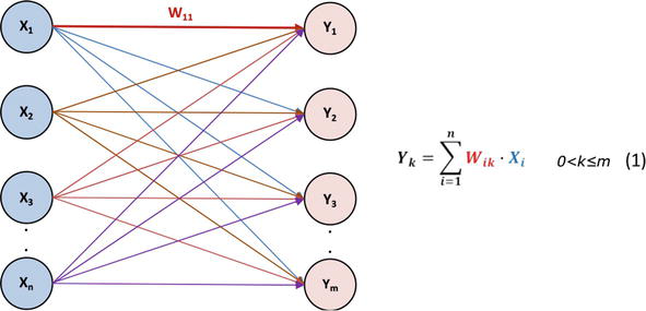
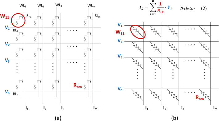
The fully connected neuromorphic network is the neuromemristive network topology that has been mostly explored in the literature [2, 30]. In this network, each neuron of a layer is connected to every neuron of the previous layer [11]. For clarity, a fully connected neuromorphic network made of two layers is considered in Figure 2. This feed-forward network can achieve classification tasks based on a linear predictor function associating a set of weights, Wik, with an input vector, Xi. A vector-matrix multiplication is implemented to calculate outputs Yk (Eq. 1 in Figure 2) [41]. An OxRAM cell array could naturally achieve matrix–vector multiplications in one iteration. This approach has been successfully applied experimentally in [42] using a 1T1R array of metal-oxide devices used for pattern identification. Figure 3a presents how the neuromorphic network can be mapped to a classical 1T1R array. Cells in a row are organized by attaching the transistor source nodes to the Source Line (SL) and attaching transistor gate nodes to the same Word Line (WL), while the cells in a column are arranged by attaching the top electrode of the RRAM to the bit line (BL). Input vectors (Xx) are associated with input voltages (Vx), and matrix weights (Wik) are associated with memory cell resistance values Rik, provided that the ON resistance of the select transistors can be neglected compared to the OxRAM HRS/LRS resistances. This construction can achieve vector-matrix multiplications according to Eq. 2 in Figure 3. The weighted sum is calculated by determining the total current Ik and applying an activation function to the overall current. Crossbar arrays are also considered as good candidates for implementing neuromorphic networks. The structure presented in Figure 3b straightforwardly implements vector-matrix multiplication without the need for select transistors. This approach has been demonstrated experimentally in [43]. However, due to the sneak-path issues, only a 12 × 12 crossbar array size was considered [44].
Figure 2.
Two-layer feed-forward neuromorphic network.
Figure 3.
(a) Matrix–vector multiplication in a 1T1R OxRAM array and (b) in 1R crossbar array.
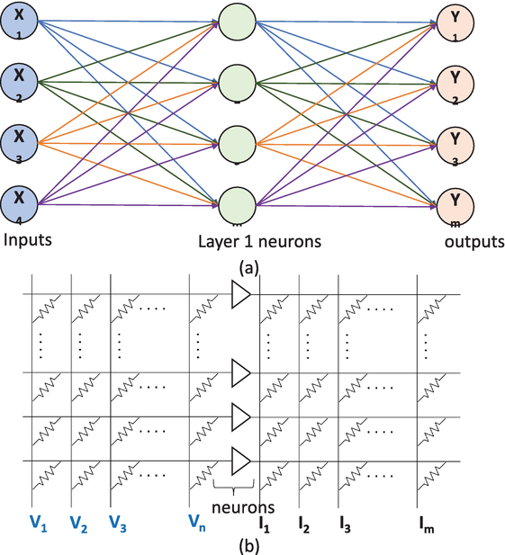
Figure 4a shows a multi-layer perceptron architecture including one hidden layer made of neurons. Figure 4b illustrates how this network can be mapped to a crossbar array. In this configuration, neurons [11] are usually designed using standard CMOS technologies. The neuron computes the weighted sum of its inputs (input vectors Xi) and applies an activation function to obtain a signal, which is conveyed to the next stage (outputs Yk).
Figure 4.
(a) Multi-layer neuromorphic network with one hidden layer and (b) mapping of the multi-layer neuromorphic network into a crossbar array.
For each network architecture, the key point is the ability of the OxRAM device to provide multiple resistance values to store synaptic weights. Indeed, before the inference stage where vector-matrix multiplication algorithms are executed, a set of weights are loaded into the network. In this stage, all the OxRAM cells of the network are programmed to a precise conductance level with respect to the pre-defined weights. Hence, the evaluation of the conductance modulation capability of OxRAM devices in a neuromorphic network context is of the prime importance.
To change OxRAM cells’ conductance values, two different approaches are considered. The first one is based on controlling the maximum voltage during the RST operation [45], and the second one is based on compliance current modulation during the SET operation [4]. Indeed, the RST programming step is a voltage-dependent process, whereas the SET programming step is a current-dependent process [4]. Another technique consisting in changing the pulse width of RST and SET voltages is also considered [18] but is not developed in this chapter. To evaluate the two above-mentioned methods, a dedicated test chip is considered for measurements.
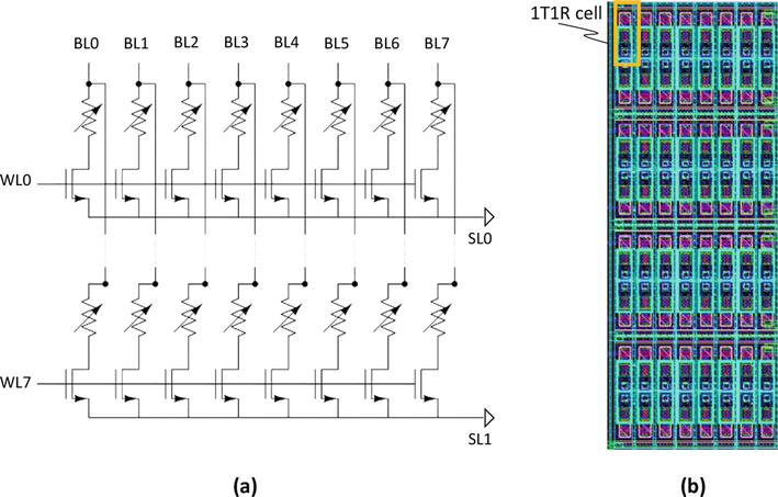
3.1 Test chip presentation and experimental setup
Figure 5 shows the schematic view of the test chip used for measurements. OxRAM cells are arranged to form eight 8-bit memory words. The active row is selected through the Word Line (WLX) signal. During a SET operation, bit line (BLX) signals are used to select specific columns. During an RST operation, signals applied to Source Lines (SLX) are used to RST a whole word or a specific cell. BL, WL, and SL nodes are externally available in order to allow a full flexibility during characterization. Measurements are performed using a Keysight B1500 semi-conductor parameter analyzer [26]. During characterization, RLRS and RHRS extraction is conducted using 1 ms voltage sweeps: the applied voltage increases step by step, and the current flowing through the cell is measured. Figure 5b presents a layout view of the memory array. Due to the limited pin out of the probe card, a subset of the 8x8 memory array is used for our experiments (7 × 7 memory array).
Figure 5.
(a) 8 × 8 OxRAM memory array and (b) layout of the memory array fabricated in a 130 nm technology.
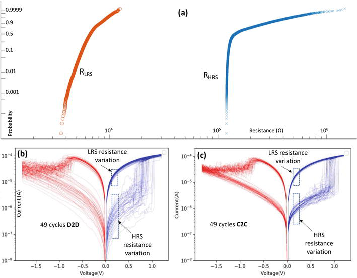
Preliminary results show that the memory array electrical characteristics are affected by variability. Figure 6 shows RHRS and RLRS distributions. 100 consecutive RST/SET operations applied to the memory array (49 cells × 100) are performed to obtain these distributions. Impact of the variability on HRS and LRS is clearly visible with an HRS distribution spread more marked with respect to the LRS one. RHRS and RLRS distributions are extracted using the following measurement protocol: before any operation, the memory array is first formed. Then, memory cells are RST one by one to extract the RHRS value at 0.1 V. After RST, cells are SET to extract the RLRS value, also at 0.1 V. The RST/SET process is repeated 100 times to obtain the resistance distributions. C2C and D2D variabilities are also revealed at the I–V characteristic level after an RST/SET operation is applied to each of the 49 cells of the memory to catch D2D variability (Figure 6b) and after an RST/SET operation is applied 49 times to an isolated cell to catch C2C variability (Figure 6c). HRS and LRS resistance values are both affected by C2C and D2D variabilities, with a more marked impact in the HRS state, particularly for D2D variability. As a conclusion, these preliminary results show that the variability, due to the inherent nature of OxRAM devices, has to be considered when designing OxRAM-based neuromorphic networks.
Figure 6.
(a) OxRAM HRS and LRS resistance distributions. OxRAM I–V characteristics highlighting (b) D2D and (c) C2C variabilities.
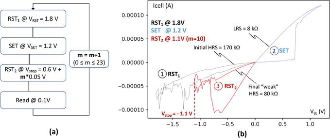
3.2 RST voltage control
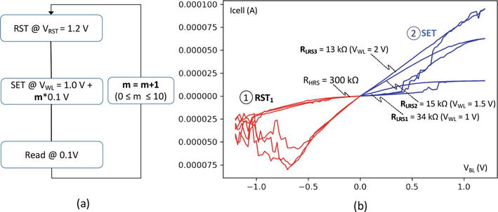
Different RST voltage biases can be applied to an OxRAM cell to control its resistance. Higher RST voltages result in higher resistance levels, while lower RST voltages lead to lower resistance levels. In our experiment, the conductance modulation is achieved by controlling the peak RST voltage referred to as Vstop. The measurement protocol is presented in Figure 7a. The protocol starts with the first RST operation (RST1) at 1.8 V peak voltage in order to set the cell in a steady HRS state. Then, a SET operation at 1.2 V peak voltage is performed to switch the cell to the LRS state. A second RST operation (RST2) with an increasing Vstop voltage is applied to the cell. Vstop ranges from 0.6 V to 1.75 V, with a 0.05 V voltage step in each iteration (24 different maximum Vstop peak voltages are considered). In each iteration, the HRS resistance variation is evaluated during a read operation. In Figure 7b, I–V curves are presented for a single cell located in the middle of the memory array. I–V characteristics are extracted following the RST1-SET-RST2 programming sequence with a Vstop value equals to 1.1 V. The initial state of the cell is a “weak” RST state before the first RST1 programming operation. The RST1 operation results in a contracted I-V hysteresis (black curve, numbered 1). From this initial HRS state (170 kΩ), a SET programming operation (blue curve, numbered 2) switches the cell to an LRS state (8 kΩ). Lastly, a “weak” RST operation, with Vstop equals to 1.1 V is applied to switch back the cell to an intermediate HRS state (red curve, numbered 3). In fact, as the RST operation is not entirely finalized due to the clamping value Vstop, the OxRAM cell ends up in an intermediate HRS resistance state (80 kΩ).
Figure 7.
(a) RHRS modulation protocol and (b) resulting I–V characteristics.
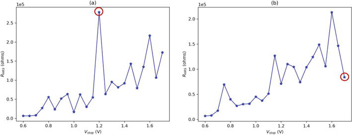
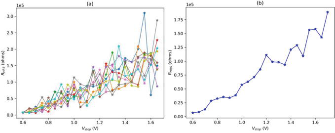
RHRS(Vstop) plot is presented in Figure 8 for two single cells. We can see that RHRS(Vstop) is not a monotonically increasing function of Vstop. The curve shows some abrupt resistance changes: resistance increase and resistance drops, both highlighted with red circles in Figure 8a and b, respectively.
Figure 8.
(a) RHRS(Vstop) for a single cell and (b) RHRS(Vstop) for a different cell, emphasizing the non-linearity of RHRS(Vstop).
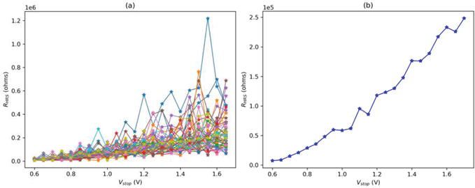
Figure 9a presents the evolution of RHRS(Vstop) for a single cell cycled 10 times to highlight C2C variability. An increasing trend of RHRS(Vstop) is observed, combined with a high variability. This increasing trend is verified in Figure 9b, which presents a curve resulting from an averaging performed on the 10 curves presented in Figure 9a. Also, for each Vstop value, the measurement protocol of Figure 7a is applied to all the cells of the memory array (49 curves) in order to catch D2D variability. An important variability is also observed (see Figure 10a). This variability is mitigated after averaging the 49 curves (see Figure 10b). Note that whether considering C2C or D2D variability, the averaging still provides a non-monotonic function of RHRS(Vstop).
Figure 9.
(a) RHRS(Vstop) for a single cell cycled 10 times (C2C variability). (b) Average curve computed from the 10 curves presented in (a).
Figure 10.
(a) RHRS(Vstop) for 49 single cells (D2D variability). (b) Average plot computed from the 49 curves presented in (a).
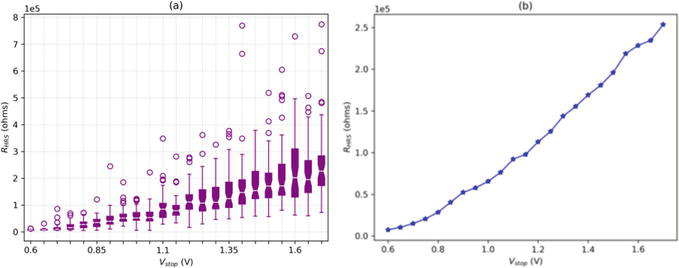
The C2C and D2D variability impact on RHRS is observed in Figure 11a, with box plots related to the same memory array programmed 10 times (box plots made of 49x10 measurements for each Vstop values). For this latter case, Figure 11b shows that the smoothing effect due to the averaging alleviates the variability: the median value of RHRS(Vstop) is turned monotonic, meaning that the mean value of RHRS strictly increases with increasing Vstop values.
Figure 11.
(a) RHRS(Vstop) box plots. Each box plot includes 49 × 10 measurements (C2C and D2D variabilities) for each Vstop value. (b) RHRS mean value vs. Vstop obtained from box plots presented in (a).
These experimental results clearly show that the impact of variability on memristive ANN parameters, such as accuracy, requires to be evaluated if the conductance modulation is achieved using RST voltage control.
3.3 Compliance current modulation during SET
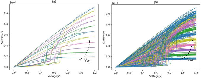
Conductance modulation in OxRAM can also be achieved by changing the compliance current IC, where IC refers to the maximum current allowed to flow through the cell during the SET operation. Indeed, it has been demonstrated that the final cell resistance is a function of IC [28]. Higher IC values lower the LRS resistance, while lower IC values increase the LRS resistance. In the 1T1R cell, the current involved in the SET operation is controlled by changing the gate transistor voltage VWL (see Figure 1a). The compliance current modulation measurement protocol is presented in Figure 12a. First, OxRAM cells are RST to start from a nominal HRS state. After RST, a SET operation is achieved with a variable VWL voltage (“weak” SET) to enter the LRS state. VWL ranges from 1 V to 2 V, with a 0.1 V voltage step in each iteration, giving 11 distinct VWL voltage levels. In each iteration, the LRS resistance is measured during a read operation.
Figure 12.
(a) Compliance current modulation measurement protocol and (b) RLRS(VWL) for three different VWL values (2 V, 1.5 V and 1 V).
Figure 12b shows the effect of three different VWL voltage levels (2 V, 1.5 V, and 1 V) on a single cell. When VWL decreases, the maximum SET current decreases, resulting in three distinctive LRS levels (13 kΩ, 15 kΩ, and 34 kΩ), while the HRS resistance stays in the same range with a value of around 300 kΩ. The evolution of RLRS(VWL) is presented in Figure 13a for increasing VWL values (one single cell is considered). An increase of RLRS (i.e., current slope increase) is clearly visible. Figure 13b presents the evolution of the LRS current versus VWL while considering D2D variability. A straight impact of variability on the different LRS resistance levels is clearly visible.
Figure 13.
(a) RLRS(VWL) for 11 VWL voltage values. (b) Effect of D2D variability on RLRS(VWL) plots.
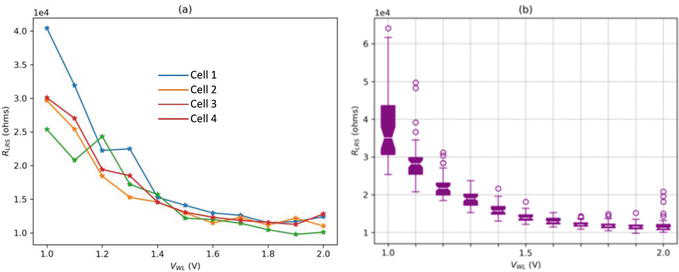
Figure 14a considers four isolated cells and shows that RLRS(VWL) is not a monotonic function of VWL. Yet, resistance drops are less marked compared to the RST voltage approach (Figure 10a). Figure 14b shows a box plot representation of RLRS(VWL) for all the memory array cells (49 measurements for each VWL level). The higher the select transistor gate voltage value, the lower the RLRS after SET. Furthermore, for low VWL values, RLRS values are more spread. Conversely, when the compliance current IC is high, the SET operation is more efficient, generating tighter distributions [29].
Figure 14.
(a) RLRS(VWL) for four isolated cells and (b) RLRS(VWL) box plots. Each box plot gathers 49 measurements.
In both compliance current and RST voltage control approaches, the idea was to define a relationship between the SET compliance current and the RST voltage versus RHRS or RLRS, respectively. RHRS or RLRS variations were expected to follow a monotonic evolution to confidently implement a consistent conductance modulation scheme. In this context, the proposed study shows that the variability of OxRAM technology results in resistance variations not easily compatible with the neuromorphic network architecture design.
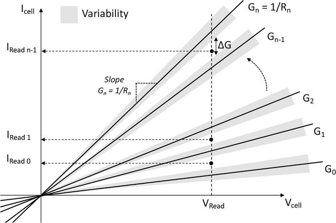
At the cell level, the conductance modulation can be seen as a segmentation of the current-voltage plane by different I-V line segments. For simplicity, only 8 I-V characteristics are presented in Figure 15. Each characteristic has a slope of Gx equals to 1/Rx, where x represents the number of resistance states ranging from 0 to n. Figure 15 shows that a reliable conductance modulation strategy does not just depend on the programming operation but also depend on an accurate read mechanism. As already mentioned in the introduction, a read operation is conducted by applying a low bit line voltage bias VRead to the OxRAM cell transistor and sensing the resulting currents referred to as IRead 0 to IRead n-1. Each current reflects the OxRAM conductance value. Several parameters, including variability, can impact the conductance margin ΔG and ultimately result in I-V characteristic overlaps. To consider the variability of the n HRS/LRS resistance states, a conductance margin, represented by shaded strips encompassing each I-V characteristic, is added in Figure 15.
Figure 15.
I–V plane segmentation after a programming operation. Variability is illustrated by a shaded area encompassing each I–V characteristic. During a read operation, the OxRAM select transistor gate is biased (VRead voltage), and different currents IRead are sensed.
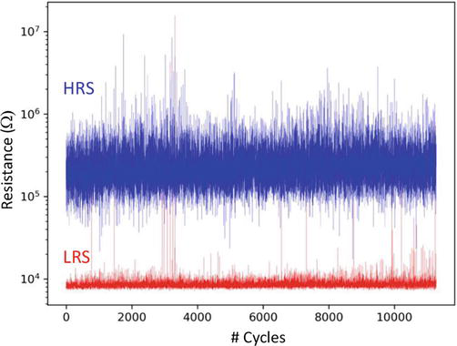
In addition to variability, another important limitation needs to be considered for the reliable use of OxRAM in neuromorphic network architectures. This limitation is known as soft errors. A soft error is a random and non-permanent upsetting of the data stored in a memory cell, in contrast to a hard error, which is a non-recoverable failure of a cell. It has been demonstrated that OxRAM resistance can get unpredictably stuck at one resistance state for some time and suddenly recover the normal operation. Figure 16 presents the evolution of RHRS and RLRS extracted at 0.1 V versus the number of programming cycles. Each programming cycle ranges from 0 to 11,269. When analyzing Figure 16, many HRS and LRS level overlaps are clearly visible. These overlaps happen either because one cell stops meeting its nominal characteristics or because one cell is stuck at a resistance state for one or several cycles before recovering. However, no specific pattern has been detected, demonstrating the unpredictable nature of the OxRAM technology.
Figure 16.
RHRS/RLRS in log scale over 200 and 30 cycles applied to the 7 × 7 memory array.
These overlaps can be explained from a physical standpoint. If during a SET operation too many bonds between some of the metal and oxygen ions in the oxide layer break, too many oxygen ions are attracted to the top electrode, hence leaving oxygen vacancies acting as a conductive filament (CF). Therefore, the voltage applied across the cell to induce an effective RST operation might not be high enough. In such a case, switching the cell may demand several programming cycles in order to get those oxygen ions to drift back [46]. Conversely, if during an RST operation too many ions are displaced, the voltage needed to induce an efficient SET operation in the next programming cycle may not be sufficient, leading the device to be stuck at HRS for several cycles [47, 48]. To mitigate soft error impact on memristive networks, it is necessary to design specific circuits able to monitor the effectiveness of each RST/SET operation [18, 49]. Also, it has a been reported at the memory array level that during consecutive RST/SET operations, write disturb can occur and impact the performance of the memory cells. The write disturb occurs when a neighboring memory cell is affected or altered during a write operation applied to a specific memory cell, leading to inadvertent resistance changes [50]. Moreover, over time, a typical bottleneck for OxRAMs lies in the endurance and retention reliability issues. These two reliability metrics narrow the resistance window, hence reducing significantly the conductance modulation capability [51, 52]. Note that cycling and endurance can lead to hard errors (memory cell stuck at one state forever). Likewise to other emerging memory technologies, OxRAM is inclined to defects [53] due to manufacturing conditions. Hence, appropriate test strategies are required to detect OxRAM-related failures [54]. However, in addition to conventional faults, OxRAM, due to its specific manufacturing process and switching mechanism, can be impacted by unique faults such as over-forming and undefined state faults [55]. Therefore, a complete fault analysis methodology needs to be defined for this memory class. Alternatively, OxRAM memristive networks have the potential to be used in harsh spatial environments [56, 57]. In such conditions, there are certain considerations and challenges that need to be addressed for OxRAM to operate reliably, such as high levels of radiations, including ionizing particles [58, 59]. These radiations can cause unwanted effects, such as resistance drifts during the OxRAM device operation [12]. To mitigate theses effects, OxRAM devices need to be radiation-hardened or shielded [12].
This study assesses the potential of OxRAMs to offer different conductance levels. The study evaluates two different programming schemes: RST voltage modulation and SET current modulation. Measurement results have established that the two programming approaches provide resistance levels highly affected by variability, which prevents an accurate control of OxRAM resistances. The RST voltage control approach shows high variability. The SET current control approach shows a more contained variability. However, in the latter approach, the variability grows exponentially with decreasing compliance currents. According to the presented experimental results, variability appears to be the main hurdle for OxRAMs used in ANN. Indeed, these systems rely on training algorithms to adjust the synaptic weights and optimize the network performances. Variability in OxRAMs can affect the convergence of these algorithms. As the device exhibits different characteristics, the learning stage might become challenging, although techniques such as adaptive learning algorithms and training strategies that account for device variability can help address this limitation. Moreover, for OxRAM technologies suffering from limited endurance, frequent updates of synaptic weights during training become even more challenging. However, ongoing research tries to address all these challenges as advanced device designs, materials engineering, circuit techniques, and system-level optimizations are being explored to improve the performance, reliability, and energy efficiency of OxRAM-based neuromemristive systems.
References
1.Aziza H. Embedded memories. In: Chapter 7 in Silicon Systems for Wireless Lan 22. World Scientific; 2020. p. 199. DOI: 10.1142/9789811210723_0007
2.Lee Y-L, Tsung P-K, Wu M. Techology trend of edge AI. In: Symposium on VLSI Design, Automation and Test (VLSI-DAT). IEEE; 2018. DOI: 10.1109/VLSI-DAT.2018.8373244
3.Shimeng Y, Chen P-Y. Emerging memory technologies: Recent trends and prospects. IEEE Solid-State Circuits Magazine. 2016;8(2):43-56. DOI: 10.1109/MSSC.2016.2546199
4.Ielmini D. Resistive switching memories based on metal oxides: Mechanisms, reliability and scaling. Semiconductor Science and Technology. 2016;31(6):1-25. DOI: 10.1088/0268-1242/31/6/063002
5.Linn E et al. Logic operations in passive crossbar arrays alongside memory operations. Nanotechnology. 2012;23(30):305205. DOI: 10.1088/0957-4484/23/30/305205
6.Roy D et al. Neural networks at the edge. In: 2019 IEEE International Conference on Smart Computing (SMARTCOMP). IEEE; 2019. pp. 45-50. DOI: 10.1109/SMARTCOMP.2019.00027
7.Indiveri G et al. Neuromorphic silicon neuron circuits. Frontiers in Neuroscience. 2011;5:73. DOI: 10.3389/fnins.2011.00073
8.Bi G-q, Poo M-m. Synaptic modifications in cultured hippocampal neurons: Dependence on spike timing, synaptic strength, and postsynaptic cell type. The Journal of Neuroscience. 1998;18(24):10 464-10 472. DOI: 10.1523/JNEUROSCI
9.Vatajelu EI et al. Nonvolatile memories: Present and future challenges. In: Design & Test Symposium (IDT), 2014 9th International. IEEE; 2014. pp. 61-66. DOI: 10.1109/IDT.2014.7038588
10.Bazzi H et al. RRAM-based non-volatile SRAM cell architectures for ultra-low-power applications. Analog Integrated Circuits and Signal Processing. 2021;106:351-361. DOI: 10.1007/s10470-020-01587-z
11.Aziza H et al. A capacitor-less CMOS neuron circuit for neuromemristive networks. In: 2019 17th IEEE International New Circuits and Systems Conference (NEWCAS). IEEE; 2019. DOI: 10.1109/NEWCAS44328.2019.8961278
12.Vaz PI et al. Improving TID radiation robustness of a CMOS OxRAM-based neuron circuit by using enclosed layout transistors. IEEE Transactions on Very Large Scale Integration (VLSI) Systems. 2021;29(6):1122-1131. DOI: 10.1109/TVLSI.2021.3067446
13.Aziza H et al. An augmented OxRAM synapse for spiking neural network (SNN) circuits. In: 2019 14th International Conference on Design & Technology of Integrated Systems in Nanoscale Era (DTIS). IEEE; 2019. pp. 1-5. DOI: 10.1109/DTIS.2019.8735057
14.Aziza H, Hamdioui S, Fieback M, Taouil M, Moreau M. Density enhancement of RRAMs using a RESET write termination for MLC operation. In: 2021 Design, Automation & Test in Europe Conference & Exhibition (DATE). Grenoble, France: IEEE; 2021. pp. 1877-1880. DOI: 10.23919/DATE51398.2021.9473967
15.Luo Y, Han X, Ye Z, Barnaby H, Seo J-S, Yu S. Array-level programming of 3-bit per cell resistive memory and its application for deep neural network inference. IEEE Transactions on Electron Devices. 2020;67(11):4621-4625. DOI: 10.1109/TED.2020.3015940
16.Milo V et al. Accurate program/Verify schemes of resistive switching memory (RRAM) for In-memory neural network circuits. IEEE Transactions on Electron Devices. 2021;68(8):3832-3837. DOI: 10.1109/TED.2021.3089995
17.Woo J, Moon K, Song J, Kwak M, Park J, Hwang H. Optimized programming scheme enabling linear potentiation in filamentary HfO2 RRAM synapse for neuromorphic systems. IEEE Transactions on Electron Devices. 2016;63(12):5064-5067. DOI: 10.1109/TED.2016.2615648
18.Zhao L et al. Improved multi-level control of RRAM using pulse-train programming. In: IEEE International Symposium on VLSI Technology, Systems and Application (VLSI-TSA). IEEE; 2014. DOI: 10.1109/VLSI-TSA.2014.6839673
19.Wang Y et al. Investigation of resistive switching in Cu-doped HfO2 thin film for multilevel non-volatile memory applications. Nanotechnology. 2009;21(4):045202. DOI: 10.1088/0957-4484/21/4/045202
20.Freitas P, Chai Z, Zhang W, Zhang JF, Marsland J. Impact of RTN and variability on RRAM-based neural network. In: 2020 IEEE 15th International Conference on Solid-State & Integrated Circuit Technology (ICSICT). Kunming, China; 2020. pp. 1-4. DOI: 10.1109/ICSICT49897.2020.9278290
21.Mohan C, Camuñas-Mesa LA, De La Rosa JM, Vianello E, Serrano-Gotarredona T, Linares-Barranco B. Neuromorphic low-power inference on Memristive crossbars with on-Chip offset calibration. IEEE Access. 2021;9:38043-38061. DOI: 10.1109/ACCESS.2021.3063437
22.Grossi A et al. Fundamental variability limits of filament-based RRAM. In: 2016 IEEE International Electron Devices Meeting (IEDM). 2016. pp. 4.7.1-4.7.4. DOI: 10.1109/IEDM.2016.7838348
23.Chakrabarti B et al. Multilevel switching in forming-free resistive memory devices with atomic layer deposited HfTiOx nanolaminate. IEEE Electron Device Letters. 2013;34(7):867-869. DOI: 10.1109/LED.2013.2262917
24.Aziza H, Bocquet M, Portal J-M, Muller C. Evaluation of OxRAM cell variability impact on memory performances through electrical simulations. In: 2011 11th Annual Non-Volatile Memory Technology Symposium Proceeding. IEEE; 2011. pp. 1-5. DOI: 10.1109/NVMTS.2011.6137089
25.Hajri B, Aziza H, Mansour MM, Chehab A. RRAM device models: A comparative analysis with experimental validation. IEEE Access. 2019;7:168963-168980. DOI: 10.1109/ACCESS.2019.2954753
26.Aziza H et al. True random number generator integration in a resistive RAM memory Array using input current limitation. IEEE Transactions on Nanotechnology. 2020;19:214-222. DOI: 10.1109/TNANO.2020.2976735
27.Postel-Pellerin J et al. True random number generation exploiting SET voltage variability in resistive RAM memory arrays. In: 2019 19th Non-Volatile Memory Technology Symposium (NVMTS). IEEE; 2019. pp. 1-5. DOI: 10.1109/NVMTS47818.2019.9043369
28.Yu S et al. Stochastic learning in oxide binary synaptic device for neuromorphic computing. Frontiers in Neuroscience. 2013;7:186. DOI: 10.1109/ISCAS.2014.6865321
29.Aziza H et al. Resistive RAMs as analog trimming elements. Solid-State Electronics. 2018;142:52-55. DOI: 10.1016/j.sse.2018.02.005
30.Papandroulidakis G. Experimental demonstration of RRAM-based computational cells for reconfigurable mixed-signal neuro-inspired circuits and systems [Doctoral thesis]. University of Southampton; 2021
31.Lee SR et al. Multi-level switching of triple-layered TaOx RRAM with excellent reliability for storage class memory. IEEE Symposium on VLSI Technology (VLSIT). 2012:71-72. DOI: 10.1109/VLSIT.2012.6242466
32.Esmanhotto E et al. High-density 3D monolithically integrated multiple 1T1R multi-level-cell for neural networks. In: 2020 IEEE International Electron Devices Meeting (IEDM). San Francisco, CA, USA: IEEE; 2020. pp. 36.5.1-36.5.4. DOI: 10.1109/IEDM13553.2020.9372019
33.Kim S, Zhou J, Lu WD. Crossbar RRAM arrays: Selector device requirements during write operation. IEEE Transactions on Electron Devices. 2014;61(8):2820-2826. DOI: 10.1109/TED.2014.2327514
34.Liang J et al. Cross-point memory array without cell selectors-device characteristics and data storage pattern dependencies. TED. 2010;57(10):2531-2538. DOI: 10.1109/TED.2010.2062187
35.Kim B, Li H. Leveraging 3D vertical RRAM to developing neuromorphic architecture for pattern classification. In: 2020 IEEE Computer Society Annual Symposium on VLSI (ISVLSI). Limassol, Cyprus: IEEE; 2020. pp. 258-263. DOI: 10.1109/ISVLSI49217.2020.00054
36.Pouyan P, Amat E, Hamdioui S, Rubio A. RRAM variability and its mitigation schemes. In: 2016 26th International Workshop on Power and Timing Modeling, Optimization and Simulation (PATMOS). Bremen, Germany: IEEE; 2016. pp. 141-146. DOI: 10.1109/PATMOS.2016.7833679
37.Baroni A et al. Low conductance state drift characterization and mitigation in resistive switching memories (RRAM) for artificial neural networks. IEEE Transactions on Device and Materials Reliability. 2022;22(3):340-347. DOI: 10.1109/TDMR.2022.3182133
38.Hajri B, Mansour MM, Chehab A, Aziza H. Oxide-based RRAM models for circuit designers: A comparative analysis. In: 2017 12th International Conference on Design & Technology of Integrated Systems in Nanoscale Era (DTIS). Palma de Mallorca, Spain: IEEE; 2017. pp. 1-6. DOI: 10.1109/DTIS.2017.7930176
39.Aziza H, Moreau M, Fieback M, Taouil M, Hamdioui S. An energy-efficient current-controlled write and read scheme for resistive RAMs (RRAMs). IEEE Access. 2020;8:137263-137274. DOI: 10.1109/ACCESS.2020.3011647
40.Liu C et al. A high accuracy and robust machine learning network for pattern recognition based on binary RRAM devices. In: 2017 International Symposium on VLSI Technology, Systems and Application (VLSI-TSA). Hsinchu, Taiwan: IEEE; 2017. pp. 1-2. DOI: 10.1109/VLSI-TSA.2017.7942472
41.Prezioso M, Merrikh-Bayat F, Hoskins BD, Adam GC, Likharev KK, Strukov DB. Training and operation of an integrated neuromorphic network based on metal-oxide memristors. Nature. 2015;521(7550):61. DOI: 10.1038/nature14441
42.Yao P et al. Face classification using electronic synapses. Nature Communications. 2017;8:15199. DOI: 10.1038/ncomms15199
44.Zidan MA, Fahmy HAH, Hussain MM, Salama KN. Memristor-based memory: The sneak paths problem and solutions. Microelectronics Journal. 2013;44(2):176-183
45.Kim W et al. 3-bit multilevel switching by deep reset phenomenon in Pt/W/TaOx/Pt-ReRAM devices. IEEE Electron Device Letters. 2016;37(5):564-567. DOI: 10.1109/LED.2016.2542879
46.Aziza H, Postel-Pellerin J, Moreau M. STATE: A test structure for rapid and reliable prediction of resistive RAM endurance. IEEE Transactions on Device and Materials Reliability. 2022;22(4):500-505. DOI: 10.1109/TDMR.2022.3213191
47.Balatti S et al. Voltage-controlled cycling endurance of HfOx-based resistive-switching memory. IEEE Transactions on Electron Devices. 2015;62(10):3365-3372
48.Aziza H, Hamdioui S, Fieback M, Taouil M, Moreau M, Girard P, et al. Multi-level control of resistive ram (rram) using a write termination to achieve 4 bits/cell in high resistance state. Electronics. 2021;10(18):2222
49.Aziza H, Coulié K, Rahajandraibe W. Design considerations towards zero-variability resistive RAMs in HRS state. In: 2021 IEEE 22nd Latin American Test Symposium (LATS). IEEE; 2021
50.Li H et al. Write disturb analyses on half-selected cells of cross-point RRAM arrays. In: 2014 IEEE International Reliability Physics Symposium. Waikoloa, HI, USA: IEEE; 2014. pp. MY.3.1-MY.3.4. DOI: 10.1109/IRPS.2014.686115
51.Lanza M et al. Standards for the characterization of endurance in resistive switching devices. ACS Nano. 2021;15(11):17214-17231
52.Rana A, Akbar T, Ismail M, et al. Endurance and cycle-to-cycle uniformity improvement in tri-layered CeO2/Ti/CeO2 resistive switching devices by changing top electrode material. Scientific Reports. 2017;7:39539
53.Fieback M, Medeiros GC, Wu L, Aziza H, Bishnoi R, Taouil M, et al. Defects, fault modeling, and test development framework for RRAMs. ACM Journal on Emerging Technologies in Computing Systems (JETC). 2022;18(3):1-26
54.Fieback M et al. Device-aware test: A new test approach towards DPPB level. In: 2019 IEEE International Test Conference (ITC). Washington, DC, USA: IEEE; 2019. pp. 1-10. DOI: 10.1109/ITC44170.2019.9000134
55.Fieback M, Medeiros GC, Gebregiorgis A, Aziza H, Taouil M, Hamdioui S. Intermittent undefined state fault in RRAMs. In: 2021 IEEE European Test Symposium (ETS). IEEE; 2021. pp. 1-6
56.Castellani-Coulie K, Toure G, Portal JM, Ginez O, Aziza H, Lesea A. Circuit effect on collection mechanisms involved in single event phenomena: Application to the response of a NMOS transistor in a 90 nm SRAM cell. IEEE Transactions on Nuclear Science. 2011;58(3):870-876
57.Castellani-Coulié K, Aziza H, Rahajandraibe W, Micolau G, Portal JM. Development of a CMOS oscillator concept for particle detection and tracking. IEEE Transactions on Nuclear Science. 2013;60(4):2450-2455. DOI: 10.1109/TNS.2013.2254723
58.Coulié K, Aziza H, Rahajandraibe W. Investigation of single event effects in a resistive RAM memory array by coupling TCAD and SPICE simulations. Journal of Electronic Testing (Springer). 2023:1-14. DOI: 10.1007/s10836-023-06068-5
59.Castellani-Coulié K, Bocquet M, Aziza H, Portal JM, Rahajandraibe W, Muller C. SPICE level analysis of single event effects in an OxRRAM cell. In: 2013 14th Latin American Test Workshop-LATW. IEEE; 2013. pp. 1-5
Written By
Hassen Aziza
Submitted: 22 July 2023Reviewed: 02 August 2023Published: 29 September 2023