
Abstract
In this work, it will be shown that the change of the microwave reflection of a semiconductor by illumination can be used to determine the photoconductivity. The reliability of the method is successfully tested by monitoring the change of the position of the sample in the microwave field compared to results calculated with a simple model. Besides, the parameters determined by the measurements agree with those for a sample with known parameters (silicon). The use of illumination with fast laser pulses makes contactless study of excess charge carrier kinetics possible. Examples are given for measurements of systems difficult to access with conventional photoconductivity measurements: an amorphous semiconductor, a-Si:H, and a semiconducting powder, TiO2.
Keywords
- microwave (photo) conductivity
- charge carrier kinetics
- semiconductor quality
- photocatalysis
- carrier lifetime
1. Introduction
The kinetics and the mobilities of charge carriers are essential for the performance of semiconductor electronic devices. These processes can be studied most appropriately by investigation of the properties of excess charge carriers. In semiconductors, it is convenient to use light to induce excess charge carriers; additionally, this yields supplementary information for light-driven devices.
In the late forties semiconductor and microwave physics got a new impact after the military development during the war. The combination of both was relatively rare until, again, military interest was awakened for the investigation of coatings for airplanes, making them invisible for RADAR. This requires materials absorbing but not reflecting microwaves.
In the seventies, a radiation chemistry group in Delft (The Netherlands) published quantitative measurements of the excess conductivity excited by short electron pulses by microwave reflection in a closed waveguide system. This research initially involved the investigation of liquids and gases or solids that can be frozen from the liquid and so perfectly fit the waveguide. The dependence of the signal on the microwave frequency was used to test and to obtain quantitative results [1, 2].
In this work, the transient absorption of excess charge carriers in semiconductors in the microwave frequency range is investigated. This is performed by illumination of a sample with short laser pulses and monitoring the relative change of the microwave power reflected by the sample upon illumination, called the Time-Resolved Microwave Conductivity (TRMC) signal. This relative change is proportional to the transient conductivity, and so gives access to excess charge kinetics. A measurement configuration is used without strong requirements for the shape of the sample.
The experiments should be performed in waveguide equipment. Other experimental realizations, e.g., coaxial, appeared to be more noisy. Signals are induced by 10 ns (FWHM) pulses of an Nd:YAG laser at 1064 nm, 532 nm, and 266 nm.
Microwaves, provided by a Gunn diode, are directed to port 1 of a circulator, leading the microwaves via port 2 to the sample. The reflected microwaves are guided via port 3 to a point contact diode for transient measurements, replaced by a power head for stationary measurements. So measurements of the change of the reflected microwave power upon (pulsed) illumination can be monitored. For quantitative measurements, the sample is clamped between a variable short circuit. (a metal plate completely reflecting the microwaves that can be displaced). The TRMC signal, i.e., the relative change of the reflected microwave power upon illumination, ΔP/P, is proportional to the photo conductance ΔS(t)
where A is the sensitivity constant, Δσ is the photoconductivity, and d is the thickness of the sample.
The (dark) conductivity can be measured by measuring the reflection of the sample using the power head for detection and numerical evaluation.
In both cases, the position of the sample in the microwave field can be changed by shifting the position of the short circuit. This is very useful to test the reliability of the measurements and of the evaluation.
The equipment presented here will be described as a closed waveguide system, with the sample exactly fitting the waveguide. So, the theoretical results must be compared to the results of the present equipment to detect the possible influence of the failing of the waveguide at the position of the sample.
2. Theory
2.1 Microwaves
The theory follows the theoretical lines of the Delft group with some changes because light excitation is used, and the samples are thin semiconductors [1, 2, 3]. The theory is developed for a closed system where the sample perfectly fits the waveguide. The field reflection coefficient is calculated starting at the short circuit (yielding the boundary condition) up to the space between sample and circulator using the evolution of the field reflection coefficient in a homogeneous medium and at the interface between two media with different optical constants to obtain the reflection coefficient between sample and the circulator. The power reflection coefficient R is given by the conjugate product of the field reflection coefficient.
The change of the power reflection coefficient under illumination of the sample ΔR(t)/R is the measurement (Time Resolved Microwave Conductivity) signal. The variable short circuit enables the displacement of the position of the sample in the microwave field. The analytical solution is intricate, and it is convenient to use numerical solutions. An example of such a simulation is given in Figure 1.
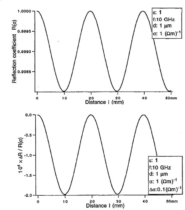
Figure 1.
Reflection coefficient R (upper curve) and ΔR/R (lower curve) in a 1-μm-thick semiconductor calculated with the model, as a function of the distance l between the short circuit and the sample (courtesy by J. Appl. Phys.).
Figure 1a shows the power reflection coefficient R as a function of the distance between the sample and the short circuit, l. The simulation has been performed for a 1 μm sample with conductivity σ = 1(Ωcm)−1, the dielectric constant ε = 1 at 10GHz. By the change of the distance l between the sample and the short circuit, the position of the sample in the sinusoidal microwave field changes: the sample is in a very small (effectively zero) microwave field if the short circuit is against the sample (at a distance zero) leading to a very small microwave absorption and a reflection coefficient unity. Displacing the short circuit from the sample leads to a decrease of the reflection coefficient up to 1 cm distance where the reflection coefficient is at a minimum, the sample is at a maximum of the microwave field, and the absorption is at maximum. At larger distances, R is the reflection coefficient increases again up to l = 2 cm. This pattern repeats, and the dependence can be characterized as the absolute value of a sinus with a period of 2 cm. This is half of the microwave wavelength at 10GHz in a waveguide. Because the conductivity is detected independently of the sign of the field, this pattern represents the microwave field.
In Figure 1b, the corresponding TRMC signals ΔR/R (or ΔP/P) are plotted for a conductivity change Δσ = 0.1(Ωcm)−1. The signal is negative (increased absorption). The highest (absolute) value of the signal is found at the minimal value of R (largest absorption) and the lowest (absolute) value at the maximum value of R (very small absorption).
2.2 (Excess) charge carrier kinetics
In Si, the (excess) conductivity is due to electrons and holes in the respective bands:
with Δn(t) (Δp(t)) the density and μn (μp) the mobility of excess electrons (holes), respectively, and e the unity charge.
In general, the decay time τ of the signal is given by:
where τs reflects decay by surface recombination and τv that due to volume recombination.
Kinetics are described by the continuity equation for electrons and that for holes connected by the Poisson equation. In crystalline silicon in most cases, the densities of electrons and holes can be considered to be equal. Then, the equations can be reduced to the ambipolar continuity equation with one diffusion constant only: the ambipolar diffusion constant. This reduces to the minority carrier diffusion constant for low injection, as it is the case for the data presented below. Detailed descriptions can be found in the literature [4].
For the present work, only some particular cases are presented. Interesting is the case of a surface that can be considered as an infinite sink for charge carriers. This can easily be tested in a silicon sample by generating a signal with 532 nm light (surface excitation). Then, the decay behavior due to recombination at the illuminated surface before an appreciable number of excess charge carriers attain the other surface is:
This extended decay is explained by the diffusion of excess charge carriers away from the recombinative surface [5].
For both surfaces abrased after uniform (1064 nm) excitation, the decay time after the establishment of a stationary (principal mode) distribution is [5]:
where D and d are the carrier diffusivity and film thickness, respectively.
For only one surface abrased, this is given by:
3. Experimental section
3.1 Measurements of silicon
3.1.1 (Dark) conductivity measurements
In Figure 2, measurements of the reflection coefficient R of a 525 μm Si wafer as a function of l are plotted (points) and compared to the best fit of the simulation with only one freely varying parameter: the conductivity σ. For this best fit, an equivalent value 47Ωcm was found to agree with the value 40-60Ωcm specified by the producer. Also, the shape of the experimental data proves that the model explains nicely the data. So, the equipment of Figure 3 can be described as a closed waveguide system as it is confirmed also by other measurements.
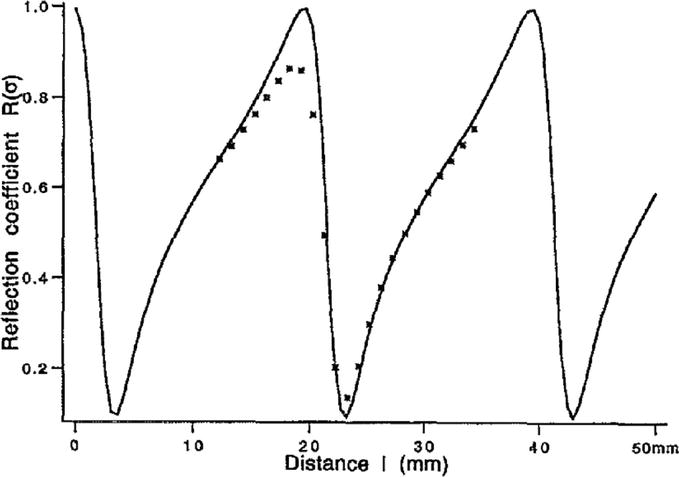
Figure 2.
Values of the reflection coefficient R measured in a 525-μm-thick n-Si wafer (40–65 Ωcm) as a function of the distance I between short circuit and the wafer (data points). The line drawn represents the best fit of the model to experimental data for σ = 2.15 (Ωcm)−1 (i.e., ρ = 47 Ωcm). (courtesy by J. Appl. Phys.).
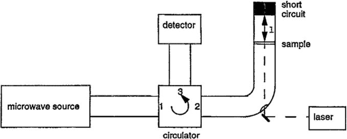
Figure 3.
Equipment for quantitative TRMC measurement.
Compared to the simulated data in Figure 1, the data in Figure 2 do not show a symmetrical shape. The presence of a material of a thickness that cannot be neglected with dielectric constant ε = 12 leads to deformation, although the signal is still periodical with 2 cm. This deformation is mainly due to the decrease of the microwave wavelength in Si.
3.1.2 An application
In Figure 4, the power reflection coefficient R as a function of the distance l between sample and short circuit is compared for a substrate p-Si wafer (100Ωcm, 500 μm) compared to data of this wafer covered at one face with 100 nm SiN and at both faces with SiN. The best fit of the data is given by the straight lines in the figure, with the conductivity as the only variable parameter.
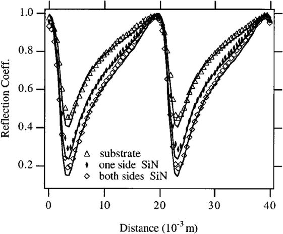
Figure 4.
The reflection coefficient R as a function of the distance l between sample and short circuit for a n-Si wafer (doping 1013 cm−3) bare, with a 100 nm SiN film on one face and a 100 nm SiN film on both faces (courtesy by Appl. Phys. Lett.).
The experimental data show good correspondence with the simulation. Evaluation of the conductivity from the simulation shows an increase of the conductivity by the presence of the SiN film and a two times higher conductivity with both faces SiN. This cannot be due to conductivity in the film; a bare SiN film does not show appreciable photoconductivity, and besides, the charge carrier mobility is very low. Consequently, the increase of the conductivity is due to an increase of charge carriers in Si. As it is known that a SiN film on Si is positively charged, these results indicate that SiN electrons are injected into Si, probably from interface states [6]. This leads to an accumulation region in Si at the interface.
For p-type Si, the same results have been obtained. Also here, a deposited SiN layer has a positive interface. In this high ohmic sample, this is due to an inversion layer in Si. So, in both cases, electrons are emitted from (defect) states in SiN to the Si substrate.
Interestingly, the dependence of this conductivity change on the thickness of the SiN layer. Measurements of the conductivity change as a function of the SiN thickness show that this change saturates at a thickness of about 20 nm (Figure 5).
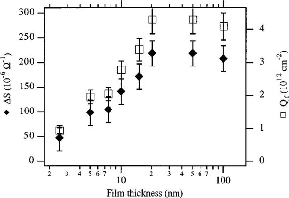
Figure 5.
Change of the conductance ΔS of a n-Si substrate as a function of the thickness of a deposited SiN film (courtesy by Appl. Phys. Lett.).
This suggests that 20 nm is sufficient for the passivation of Si by SiN as the passivation of Si by SiN is mainly due to the presence of a space charge. At higher dark conductivities, the analysis of the data is more difficult because also the role of the holes must be taken into account.
3.1.3 Photoconductivity (TRMC) measurements
First, it must be realized that the technique is not appropriate for the determination of the lifetime in state-of-the-art Si wafers, as the decay of the TRMC signal will be determined by surface recombination. However, modification of the surface, e.g., by deposition of lavers, or degradation of the volume, e.g., by radiation damage, can be studied informative measurements require the uniformity of the microwave field in the sample. So, the decay is only due to the immobilization of charge carriers and not to a change of position. This is conveniently done by comparison of the signals induced by 532 nm (surface generation) to those induced by 1064 nm (uniform generation) for the same number of photons absorbed. This shows that uniformity is at best at the maximum of the microwave field [7].
An informative impression of these effects is shown in Figure 6 for a Si wafer with abrased surfaces (i.e., infinite sinks for charge carriers):
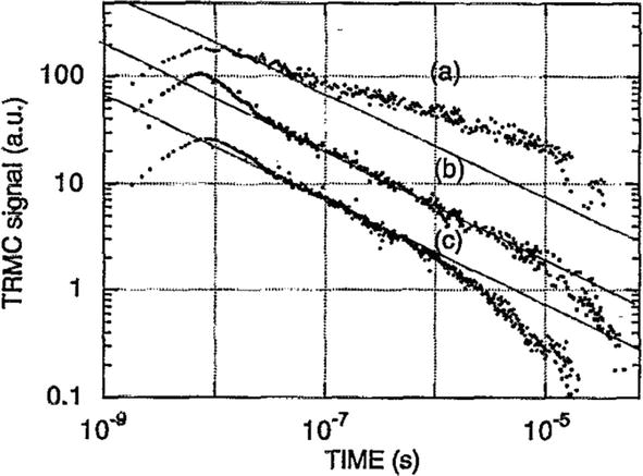
Figure 6.
TRMC transients induced by 532 nm light pulses in a 0.5 mm thick n-Si wafer (40-60Ωcm) at different distances l between the short circuit and the wafer. The label (b) refers to a position at the maximum of the microwave field, (b) and (c) to other positions. The straight lines are characterized by a slope of −0.5 (courtesy by J. Appl. Phys.).
In this figure, signals induced by 532 nm light pulses are displayed on a double logarithmic plot arbitrarily displaced in vertical direction to make the decay behavior more visible. The lines drawn have a slope 0.5: signal b was measured at the maximum of the microwave field and shows the behavior with t−0.5 as predicted by the theory (Eq. 4). It also shows the change of the slope at the time when recombination at the other surface approximately indicated by the decay time after 1064 excitation (Eq. 5). Signal a in the figure monitored at another position in the microwave field (no uniform microwave field). Here, the decay of the signal is slower due to the diffusion of charge carriers to regions in higher microwave fields. On the contrary, signal c shows a too-fast decay. Here, the charge carriers diffuse after excitation to regions with lower microwave fields. This shows the importance of a uniform microwave field to observe the real decay by charge carrier immobilization, not obscured by other effects.
3.1.4 Surface modification of silicon
In semiconductor technology, the effect of a thin surface layer on the material is very important. This can be for passivation of the surface, generation of a space charge region, or both. SiN deposited on Si obtains a positive charge and consequently induces in weakly doped p-Si an inversion layer. In Figure 7, TRMC signals induced by 532 nm light (data points) at the SiN face of a p-Si wafer only at this face covered by SiN are compared to Surface Photo Voltage signals (lines drawn) in a double logarithmic representation. SPV signals monitor the change of the voltage at the surface (in this case, over the inversion layer).
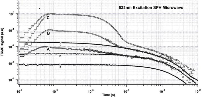
Figure 7.
TRMC transients in a p-Si wafer covered at one face by a SiN film induced by 532 nm light pulses at the covered face at different intensities. The straight line represents surface photovoltage (SPV) signals obtained under the same conditions (courtesy by Phys. Stat. Sol.).
The TRMC signals show an initially faster decay followed by a much slower decay. The SPV signals show an equivalent slow decay, but the signal is time-independent before the onset of the slow decay. The initial decay of the TRMC signal represents excess charge carriers outside the space charge region (and so invisible in SPV measurements) and shows decay at the uncovered surface given by Eq. (6).
The slow decay reflects excess charge carriers in the space charge region, generating the photo voltage observed with both methods. Consequently, TRMC measurements can be used to study kinetics in the space charge region.
Interesting is the difference between SiO and SiN covering of silicon. Both obtain a positive charge after deposition on silicon. SiN on silicon has a higher positive charge and so a larger space charge region. However, the volume decay and the decay of charge carriers in the space charge region (i.e., the decay of the photovoltage) is faster in the SiN-covered system.
3.2 Measurements of other materials
In fact, as a contactless method, the TRMC method is most appropriate for materials where the contact properties are largely unknown for all new materials. Also, for materials that cannot easily be contacted as semiconductor powders, the method seems adequate.
3.2.1 Amorphous silicon (a-Si:H)
This material has several applications in electronics. Although the application in p-i-n solar cells is limited because the degradation during extended illumination is handicapped (Staebler–Wronski effect), the use in heterojunctions is still growing strong.
Experiments were performed to verify the applicability of TRMC measurements to amorphous, low-mobility materials. A good agreement with the theory discussed above with only mobility as a varying parameter. A mobility of about 0.5cm2V−1 s−1 is obtained [8].
The transient photoconductivity in intrinsic and n-doped a-Si:H is due to electrons. The electron mobility is two orders of magnitude larger than the hole mobility, and in intrinsic a-Si:H the Fermi level is nearer to the conduction band (or in other words, it is weakly n-doped). But, even the electron mobility is only about unity, and TRMC measurements must be performed at high laser intensities.
The TRMC signal in a-Si:H after 532 nm excitation follows the pulse shape, giving way to a tail. The importance of the tail relative to the signal maximum at about 10 ns (the TRMC amplitude) increases with decreasing excitation density (Figure 8).
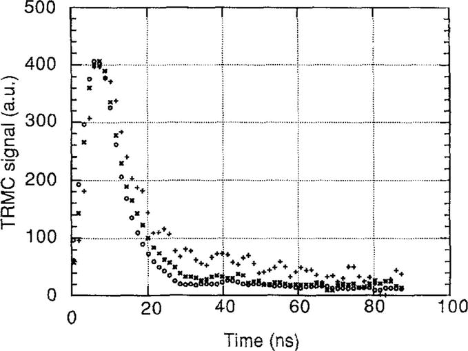
Figure 8.
TRMC transients induced by 532 nm laser pulses in an a-Si:H film at 1.5 mJ/cm2 (o), 0.15 mJ/cm2 (*) and 0.015 mJ/cm2 (+). The maxima of the TRMC amplitudes are normalized at the same value to accentuate the difference in decay behavior (permission by Appl. Phys. A).
The TRMC amplitude increases with the square root of the excitation at high excitation densities and changes in a linear dependence at low excitation densities. The square root dependence is due to a second-order electron-hole recombination already active during the excitation (Figure 8).
It appeared that even at the high excitation densities required a reliable impression of the quality of a-Si:H is obtained from the TRMC amplitude [9]. The TRMC amplitude is smaller for lesser quality material due a decrease of the mobility and trapping.
3.2.2 TiO2 powder
Titania (TiO2), a white nano-crystalline size powder, has several applications:
as a white paint, in dyes, esthetical products, etc.
as catalyst, in particular for depollution
in solar cells, covered by a dye to overcome the too-large bandgap for solar energy conversion.
TRMC measurements can elucidate the influence of surface modifications, which is important for these applications.
In Figure 9 TRMC signals are shown in a double logarithmic representation. The transient b is obtained for an untreated TiO2 (P25) sample. Treatment of the power with 2-propanol leads to a large decrease of the decay (transient a). On the contrary, treatment with tetranitromethane leads to a very large increase in decay (c). This is explained by increased electron immobilization on the tetranitromethane modified surface and an increased hole trapping at the 2-propanol modified surface.
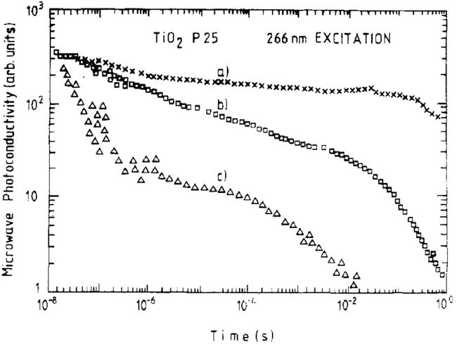
Figure 9.
TRMC signals induced by 266 nm laser pulses in TiO2 (P25) powder, (a) untreated powder, (b) treated with 2-propanol, and (c) treated with tetranitromethane (courtesy by J. Phys. Chem.).
To explain these effects it must be taken into account that the signal is due to mobile electrons. This explains the faster decay at the tetranitromethane treated surface. The trapping of holes by the 2-propanol treated surface leads to a decrease of the electron-hole recombination and so a slower electron decay and a slower TRMC decay. This experiment shows the sensitivity of TRMC measurements to the influence of surface modification on excess charge carrier kinetics. This makes the technique an important tool for the investigation of photocatalysis on semiconductor powders.
4. Conclusions
In this work it is shown that contactless measurements in the microwave frequency range yield a reliable determination of (photo)conductivity at the hand of measurements on crystalline silicon; a system with known parameters. As example, the influence of an important passivation of silicon by SiN is investigated, and injection of electrons in silicon is observed, so the positive charge of the SiN interface is explained. This leads to an accumulation layer in n-Si and a depletion/inversion layer on p-Si. Further examples concerned a-Si;H and a semiconducting powder, TiO2.
The technique is particularly appropriate for new semiconductors with unknown contacting properties [10, 11, 12] and for the investigation of powders for photocatalysis on semiconductors [13, 14].
References
- 1.
Infelta PP, de Haas MP, Warman JM. The study of the transient conductivity of pulse irradiated dielectric liquids on a nanosecond lifetime using microwaves. Radiation Physics and Chemistry. 1977; 10 :353 - 2.
de Haas MP. Thesis Leyden University. Delft: Delft University Press; 1977 - 3.
Jackson JD. Classical Electrodynamics. New York: John Wiley; 1962 - 4.
Blakemore JS. Semiconductor Statistics. Oxford: Pergamon; 1962. pp. 323-326 - 5.
Kunst M, Sanders A. Transport of excess carriers in silicon wafers. Semiconductor Science and Technology. 1992; 7 :51 - 6.
Hezel R, Schorner R. Plasma silicon nitride. A promising dielectric to achieve high-quality MIS/IL solar cells. Journal of Applied Physics. 1981; 52 :3076 - 7.
Swiatkowski C, Sanders A, Buhre KD, Kunst M. Charge carrier kinetics in semiconductors by microwave conductivity measurements. Journal of Applied Physics. 1995; 78 :1763 - 8.
Swiatkowski C, Kunst M. Characterization of amorphous silicon films by contactless transient photoconductivity measurements. Applied Physics. 1995; A61 :623 - 9.
Neitzert HC. PhD Thesis. Berlin. 1991 - 10.
Colombi G, Boshuizen B, Chaykina D, Hsu L, Schreuders H, Savenije TJ, et al. Large polaron conduction, photoconductivity and photochromism in CdOxH3-2x. Advanced Optical Materials. 2023; 11 :202202660 - 11.
Zhao J, Caselli VM, Bos M, Boshuizen B, Saqvenije TJ. How deep hole traps affect the charge dynamics and collection in bare and bilayers of methylammonium lead bromide. ACS Applied Materials and Interfaces. 2021; 13 :16309 - 12.
Guse JA, Jones TW, Danos A, McCarney DR. Recombination dynamics in thin film photovoltaic materials via time resolved microwave conductivity. Journal of Visualized Experiments. 2017; 121 :55232 - 13.
Azevedoo J, Campbell S, He D, Cornul R, Berlucchi M, Sorgues S, et al. Versatile wafer-scale technique for the formation of ultra smooth and thickness-controlled graphene oxide films based on very large flakes. ACS Applied Materials and Interfaces. 2015; 7 :21270 - 14.
Herissan A, Nawfal M, Kunst M, Colbeau-Justin C. Time resolved microwave conductivity. In: Bahnemann DW, Patrocinio AOT, editors. Studying Mobile Charge Carriers in TiO2 Photoactive Particles, Springer Handbook of Inorganic Photochemistry. Switzerland: Springer Nature; 2022